
54ACTQ841
Quiet Series 10-Bit Transparent Latch with TRI-STATE
Æ
Outputs
General Description
The 'ACTQ841 bus interface latch is designed to eliminate
the extra packages required to buffer existing latches and
provide extra data width for wider address/data paths or
buses carrying parity. The '841 is a 10-bit transparent latch,
a 10-bit version of the '373. The 'ACTQ841 utilizes NSC
Quiet Series technology to guarantee quiet output switching
and improved dynamic threshold performance, FACT Quiet
Series
TM
features GTO
TM
output control and undershoot cor-
rector in addition to a split ground bus for superior perfor-
mance.
Features
n
Guaranteed simultaneous switching noise level and
dynamic threshold performance
n
Inputs and outputs on opposite sides of package allow
easy interface with microprocessors
n
Improved latch-up immunity
n
Outputs source/sink 24 mA
n
'ACTQ841 has TTL-compatible inputs
n
Standard Microcircuit Drawing (SMD) 5962-92200
Logic Symbols
Pin Names
Description
D
0
≠D
9
Data Inputs
O
0
≠O
9
TRI-STATE Outputs
OE
Output Enable
LE
Latch Enable
GTO
TM
is a trademark of National Semiconductor Corporation.
TRI-STATE
Æ
is a registered trademark of National Semiconductor Corporation.
FACT
Æ
is a registered trademark of Fairchild Semiconductor Corporation.
FACT Quiet Series
TM
is a trademark of Fairchild Semiconductor Corporation.
DS100250-1
DS100250-2
August 1998
54ACTQ841
Quiet
Series
10-Bit
T
ransparent
Latch
with
TRI-ST
A
T
E
Outputs
© 1998 National Semiconductor Corporation
DS100250
www.national.com

Connection Diagrams
Functional Description
The 'ACTQ841 consists of ten D-type latches with
TRI-STATE outputs. The flip-flops appear transparent to the
data when Latch Enable (LE) is HIGH. This allows asynchro-
nous operation, as the output transition follows the data in
transition.
On the LE HIGH-to-LOW transition, the data that meets the
setup and hold time is latched. Data appears on the bus
when the Output Enable (OE) is LOW. When OE is HIGH the
bus output is in the high impedance state.
Function Table
Inputs
Internal
Output
Function
OE
LE
D
Q
O
X
X
X
X
Z
High Z
H
H
L
L
Z
High Z
H
H
H
H
Z
High Z
H
L
X
NC
Z
Latched
L
H
L
L
L
Transparent
L
H
H
H
H
Transparent
L
L
X
NC
NC
Latched
H = HIGH Voltage Level
L = LOW Voltage Level
X = Immaterial
Z = High Impendance
NC = No Change
Logic Diagram
Pin Assignment
for DIP and Flatpack
DS100250-3
Pin Assignment
for LCC
DS100250-4
DS100250-5
Please note that this diagram is provided only for the understanding of logic operations and should not be used to estimate propagation delays.
www.national.com
2

Absolute Maximum Ratings
(Note 1)
If Military/Aerospace specified devices are required,
please contact the National Semiconductor Sales Office/
Distributors for availability and specifications.
Supply Voltage (V
CC
)
-0.5V to +7.0V
DC Input Diode Current (I
IK
)
V
I
= -0.5V
-20 mA
V
I
= V
CC
+ 0.5V
+20 mA
DC Input Voltage (V
I
)
-0.5V to V
CC
+ 0.5V
DC Output Diode Current (I
OK
)
V
O
= -0.5V
-20 mA
V
O
= V
CC
+ 0.5V
+20 mA
DC Output Voltage (V
O
)
-0.5V to V
CC
+ 0.5V
DC Output Source
or Sink Current (I
O
)
±
50 mA
DC V
CC
or Ground Current
per Output Pin (I
CC
or I
GND
)
±
50 mA
Storage Temperature (T
STG
)
-65∞C to +150∞C
DC Latch-Up Source
or Sink Current
±
300 mA
Junction Temperature (T
J
)
CDIP
175∞C
Recommended Operating
Conditions
Supply Voltage (V
CC
)
'ACTQ
4.5V to 5.5V
Input Voltage (V
I
)
0V to V
CC
Output Voltage (V
O
)
0V to V
CC
Operating Temperature (T
A
)
54ACTQ
-55∞C to +125∞C
Minimum Input Edge Rate
V/
t
'ACTQ Devices
V
IN
from 0.8V to 2.0V
V
CC
@
4.5V, 5.5V
125 mV/ns
Note 1: Absolute maximum ratings are those values beyond which damage
to the device may occur. The databook specifications should be met, without
exception, to ensure that the system design is reliable over its power supply,
temperature, and output/input loading variables. National does not recom-
mend operation of FACT
Æ
circuits outside databook specifications.
Note 2: All outputs loaded; thresholds on input associated with output under
test.
DC Electrical Characteristics for 'ACTQ Family Devices
Symbol
Parameter
V
CC
(V)
54ACTQ
Units
Conditions
T
A
=
-55∞C to +125∞C
Guaranteed Limits
V
IH
Minimum High Level
4.5
2.0
V
V
OUT
= 0.1V
Input Voltage
5.5
2.0
or V
CC
- 0.1V
V
IL
Maximum Low Level
4.5
0.8
V
V
OUT
= 0.1V
Input Voltage
5.5
0.8
or V
CC
- 0.1V
V
OH
Minimum High Level
4.5
4.4
V
I
OUT
= -50 µA
Output Voltage
5.5
5.4
(Note 3)
V
IN
= V
IL
or V
IH
4.5
3.70
V
I
OH
= -24 mA
5.5
4.70
I
OH
= -24 mA
V
OL
Maximum Low Level
4.5
0.1
V
I
OUT
= 50 µA
Output Voltage
5.5
0.1
(Note 3)
V
IN
= V
IL
or V
IH
4.5
0.50
V
I
OL
= -24 mA
5.5
0.50
I
OL
= -24 mA
I
IN
Maximum Input
5.5
±
1.0
µA
V
I
= V
CC
, GND
Leakage Current
I
OZ
Maximum
5.5
±
10.0
µA
V
I
= V
IL
, V
IH
TRI-STATE
V
O
= V
CC
, GND
Leakage Current
I
CCT
Maximum I
CC
/Input
5.5
1.6
mA
V
I
= V
CC
- 2.1V
www.national.com
3

DC Electrical Characteristics for 'ACTQ Family Devices
(Continued)
Symbol
Parameter
V
CC
(V)
54ACTQ
Units
Conditions
T
A
=
-55∞C to +125∞C
Guaranteed Limits
I
OLD
Minimum Dynamic
5.5
50
mA
V
OLD
= 1.65V Max
I
OHD
Output Current
(Note 4)
5.5
-50
mA
V
OHD
= 3.85V Min
I
CC
Maximum Quiescent
5.5
160.0
µA
V
IN
= V
CC
Supply Current
or GND (Note 5)
V
OLP
Quiet Output
5.0
1.5
V
(Note 6)
Maximum Dynamic V
OL
V
OLV
Quiet Output
5.0
-1.2
V
(Note 6)
Minimum Dynamic V
OL
Note 3: All outputs loaded; thresholds on input associated with output under test.
Note 4: Maximum test duration 2.0 ms, one output loaded at a time.
Note 5: I
CC
for 54ACTQ
@
25∞C is identical to 74ACTQ
@
25∞C.
Note 6: Max number of outputs defined as (n). Data inputs are driven 0V to 3V. One output
@
GND.
AC Electrical Characteristics
54ACTQ
V
CC
T
A
= -55∞C
Fig.
Symbol
Parameter
(V)
to +125∞C
Units
No.
(Note 7)
C
L
= 50 pF
Min
Max
t
PLH
,
Propagation Delay
5.0
2.0
9.5
ns
Figure 4
t
PHL
D
n
to O
n
2.0
11.0
t
PLH
,
Propagation Delay
5.0
2.0
11.0
ns
Figure 4
t
PHL
LE to O
n
2.0
11.0
t
PZH
,
Output Enable Time
5.0
1.5
11.0
ns
Figure 5
t
PZL
OE to O
n
1.5
13.0
t
PHZ
,
Output Disable Time
5.0
1.5
8.5
ns
Figure 5
t
PLZ
OE to O
n
1.5
5.5
Note 7: Voltage Range 5.0 is 5.0V
±
0.5V.
Note 8: Skew is defined as the absolute value of the difference between the actual propagation delay for any two outputs within the same packaged device. The
specification applies to any outputs switching in the same direction, either HIGH to LOW (t
OSHL
) or LOW to HIGH (t
OSLH
). Parameter guaranteed by design. Not
tested.
AC Operating Requirements
54ACTQ
V
CC
T
A
= -55∞C
Fig.
Symbol
Parameter
(V)
to +125∞C
Units
No.
(Note 9)
C
L
= 50 pF
Guaranteed Minimum
t
S
Setup Time, HIGH or LOW
5.0
3.0
ns
Figure 7
D
n
to LE
t
H
Hold Time, HIGH or LOW
5.0
1.5
ns
Figure 7
D
n
to LE
t
W
LE Pulse Width, HIGH
5.0
4.0
ns
Figure 6
Note 9: Voltage Range 5.0 is 5.0V
±
0.5V.
www.national.com
4
Capacitance
Symbol
Parameter
Typ
Units
Conditions
C
IN
Input Capacitance
4.5
pF
V
CC
= OPEN
C
PD
Power Dissipation
85.0
pF
V
CC
= 5.0V
Capacitance
AC Loading
AC Waveforms
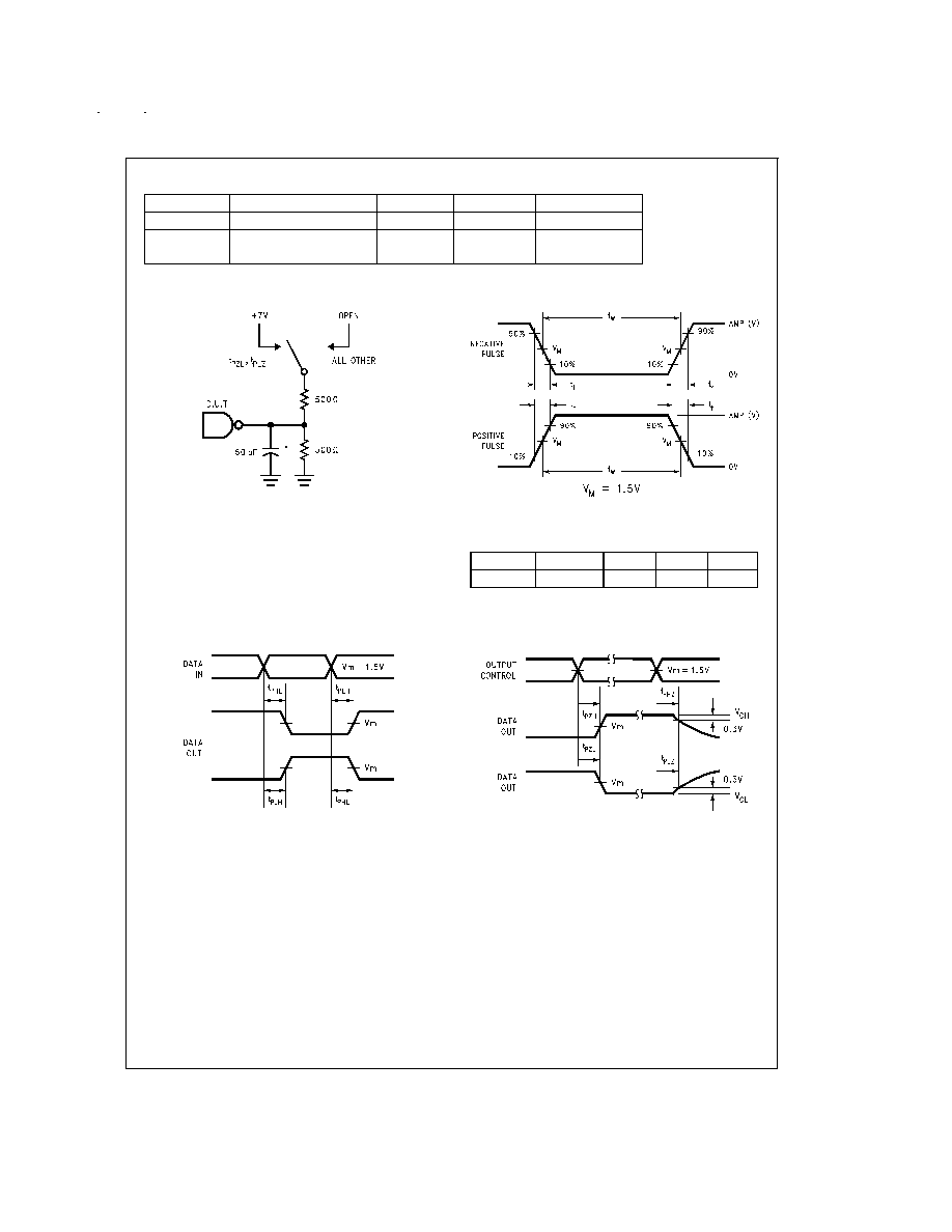
DS100250-9
*Includes jig and probe capacitance
FIGURE 1. Standard AC Test Load
DS100250-10
FIGURE 2. Test Input Signal Levels
Amplitude
Rep. Rate
t
w
t
r
t
f
3.0V
1 MHz
500 ns
2.5 ns
2.5 ns
FIGURE 3. Test Input Signal Requirements
DS100250-11
FIGURE 4. Propagation Delay Waveforms for
Inverting and Non-Inverting Functions
DS100250-13
FIGURE 5. TRI-STATE Output HIGH and LOW
Enable and Disable Time
www.national.com
5