
54F/74F109
Dual JK Positive Edge-Triggered Flip-Flop
General Description
The 'F109 consists of two high-speed, completely indepen-
dent transition clocked JK flip-flops. The clocking operation
is independent of rise and fall times of the clock waveform.
The JK design allows operation as a D flip-flop (refer to 'F74
data sheet) by connecting the J and K inputs.
Asynchronous Inputs:
LOW input to S
D
sets Q to HIGH level
LOW input to C
D
sets Q to LOW level
Clear and Set are independent of clock
Simultaneous LOW on C
D
and S
D
makes both Q and Q
HIGH
Features
n
Guaranteed 4000V minimum ESD protection.
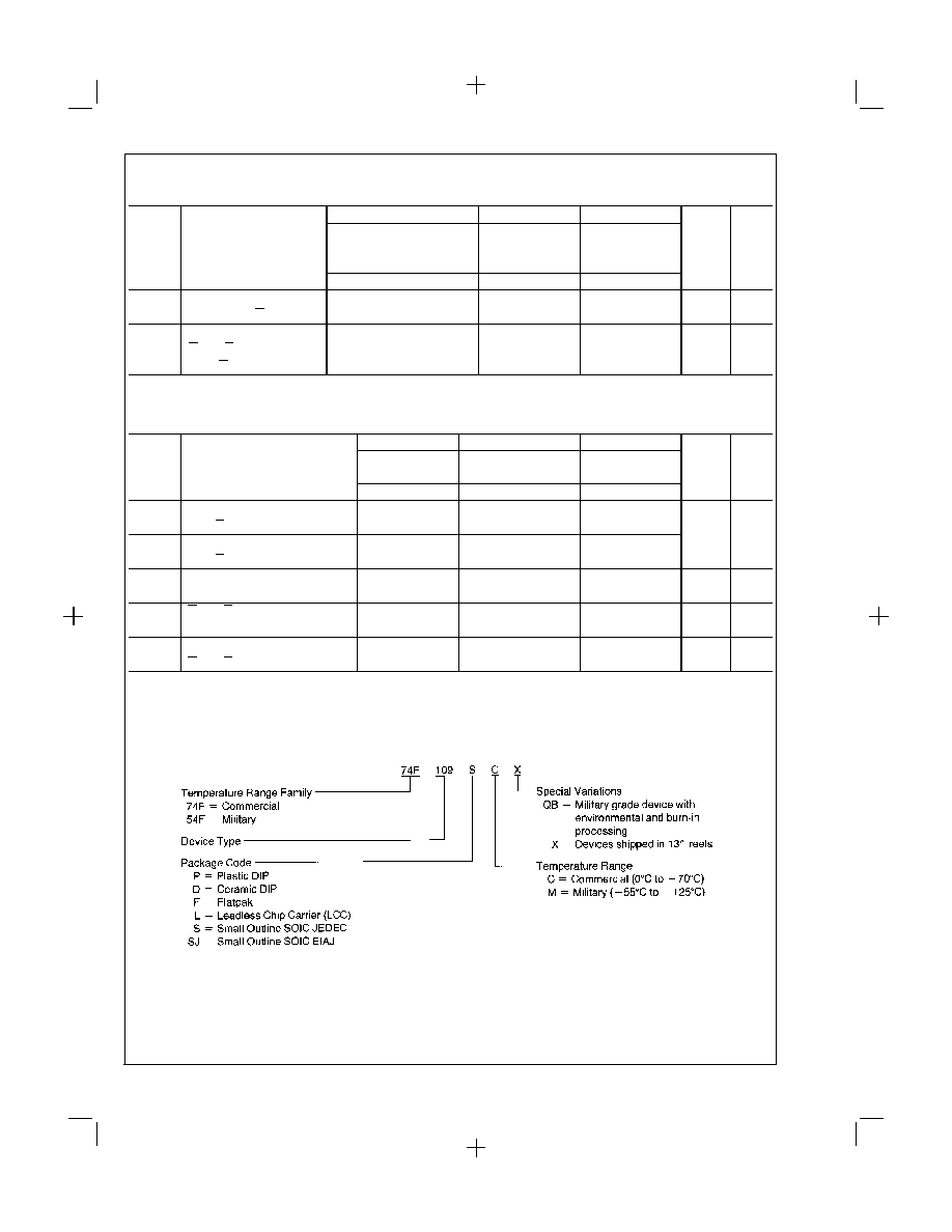
Ordering Code:
See Section 0
Commercial
Military
Package
Package Description
Number
74F109PC
N16E
16-Lead (0.300" Wide) Molded Dual-in-Line
54F109DM (Note 2)
J16A
16-Lead Ceramic Dual-in-Line
74F109SC (Note 1)
M16A
16-Lead (0.150" Wide) Molded Small Outline,
JEDEC
74F109SJ (Note 1)
M16D
16-Lead (0.300" Wide) Molded Small Outline,
EIAJ
54F109FM (Note 2)
W16A
16-Lead Cerpack
54F109LM (Note 2)
E20A
16-Lead Ceramic Leadless Chip Carrier, Type C
Note 1: Devices also available in 13" reel. Use suffix = SCX and SJX.
Note 2: Military grade device with environmental and burn-in processing. Use suffix = DMQB, FMQB and LMQB.
Logic Symbols
FAST
�
and TRI-STATE
�
are registered trademarks of National Semiconductor Corporation.
DS009471-3
DS009471-4
IEEE/IEC
DS009471-6
November 1994
54F/74F109
Dual
JK
Positive
Edge-T
riggered
Flip-Flop
54F/74F109
� 1997 National Semiconductor Corporation
DS009471
www.national.com
1
PrintDate=1997/08/28 PrintTime=11:45:22 10182 ds009471 Rev. No. 1
cmserv
Proof
1
DSXXX

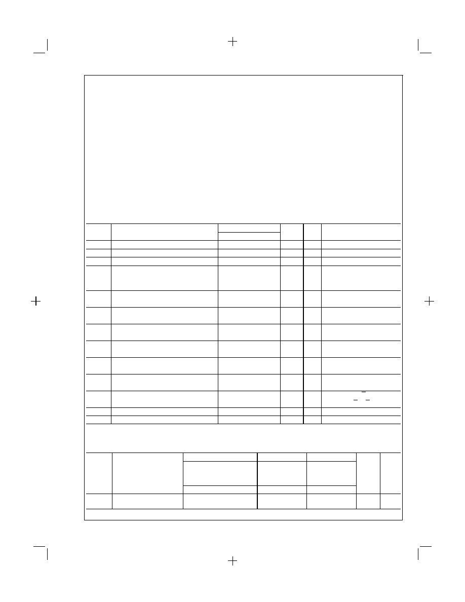
Connection Diagrams
Unit Loading/Fan Out
See Section 0 for U.L. definitions
54F/74F
Pin Names
Description
U.L.
Input I
IH
/I
IL
HIGH/LOW
Output I
OH
/I
OL
J
1
, J
2
, K
1
, K
2
Data Inputs
1.0/1.0
20 �A/-0.6 mA
CP
1
, CP
2
Clock Pulse Inputs (Active Rising Edge)
1.0/1.0
20 �A/-0.6 mA
C
D1
, C
D2
Direct Clear Inputs (Active LOW)
1.0/3.0
20 �A/-1.8 mA
S
D1
, S
D2
Direct Set Inputs (Active LOW)
1.0/3.0
20 �A/-1.8 mA
Q
1
, Q
2
, Q
1
, Q
2
Outputs
50/33.3
-1 mA/20 mA
Truth Table
Inputs
Outputs
S
D
C
D
CP
J
K
Q
Q
L
H
X
X
X
H
L
H
L
X
X
X
L
H
L
L
X
X
X
H
H
H
H
N
l
l
L
H
H
H
N
h
l
Toggle
H
H
N
l
h
Q
0
Q
0
H
H
N
h
h
H
L
H
H
L
X
X
Q
0
Q
0
H (h) = HIGH Voltage Level
L (l) = LOW Voltage Level
N
= LOW-to-HIGH Transition
X = Immaterial
Q
0
(Q
0
) = Before LOW-to-HIGH Transition of Clock
Lower case letters indicate the state of the referenced output one setup time prior to the LOW-to-HIGH clock transition.
Pin Assignment
for DIP, SOIC and Flatpak
DS009471-1
Pin Assignment
for LCC
DS009471-2
PrintDate=1997/08/28 PrintTime=11:45:23 10182 ds009471 Rev. No. 1
cmserv
Proof
2
DSXXX
www.national.com
2
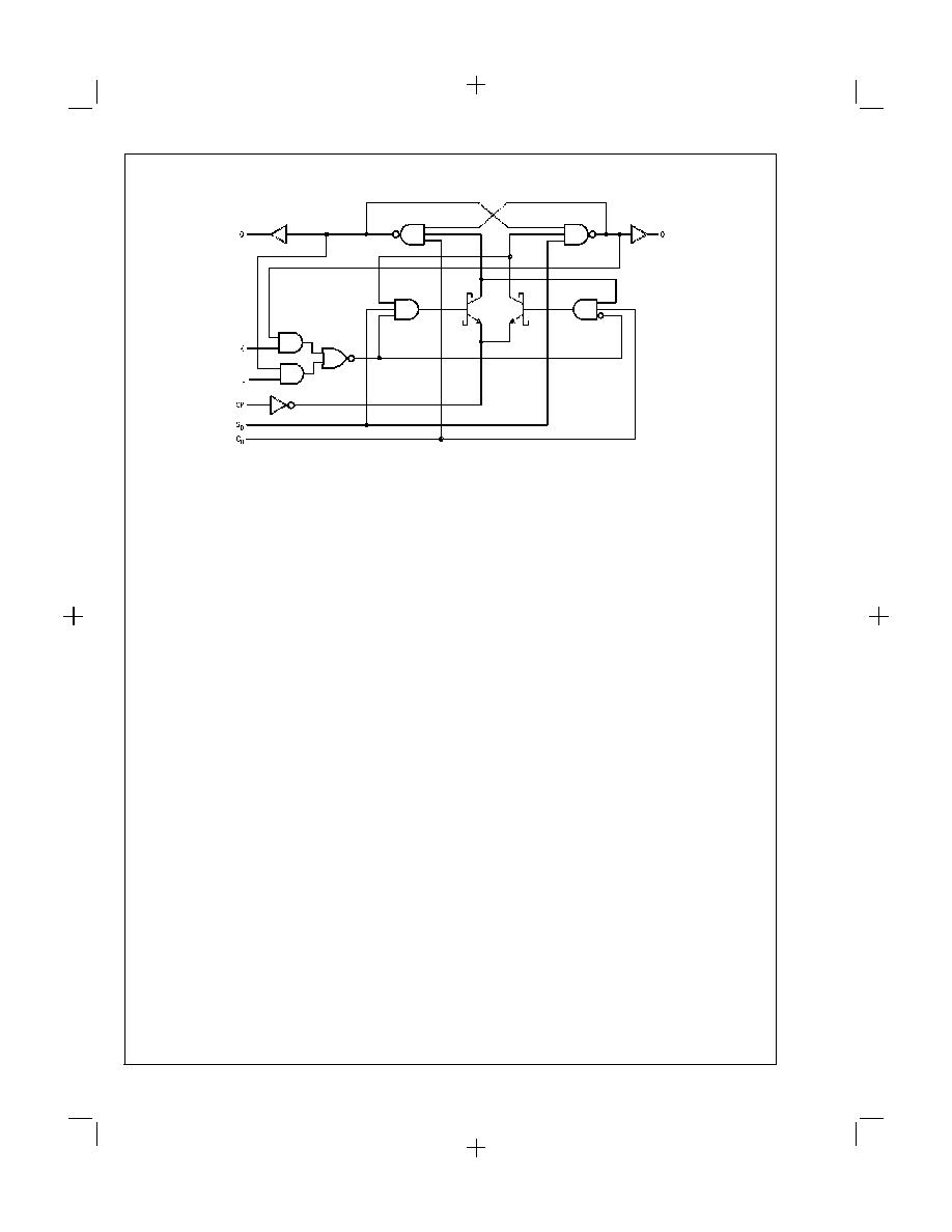
Logic Diagram
(One Half Shown)
DS009471-5
Please note that this diagram is provided only for the understanding of logic operations and should not be used to estimate propagation delays.
3
www.national.com
PrintDate=1997/08/28 PrintTime=11:45:24 10182 ds009471 Rev. No. 1
cmserv
Proof
3
Absolute Maximum Ratings
(Note 3)
If Military/Aerospace specified devices are required,
please contact the National Semiconductor Sales Office/
Distributors for availability and specifications.
Storage Temperature
-65�C to +150�C
Ambient Temperature under Bias
-55�C to +125�C
Junction Temperature under Bias
-55�C to +175�C
Plastic
-55�C to +150�C
V
CC
Pin Potential to
Ground Pin
-0.5V to +7.0V
Input Voltage (Note 4)
-0.5V to +7.0V
Input Current (Note 4)
-30 mA to +5.0 mA
Voltage Applied to Output
in HIGH State (with V
CC
= 0V)
Standard Output
-0.5V to V
CC
TRI-STATE
�
Output
-0.5V to +5.5V
Current Applied to Output
in LOW State (Max)
twice the rated I
OL
(mA)
ESD Last Passing Voltage (Min)
4000V
Recommended Operating
Conditions
Free Air Ambient Temperature
Military
-55�C to +125�C
Commercial
0�C to +70�C
Supply Voltage
Military
+4.5V to +5.5V
Commercial
+4.5V to +5.5V
Note 3: Absolute maximum ratings are values beyond which the device may
be damaged or have its useful life impaired. Functional operation under these
conditions is not implied.
Note 4: Either voltage limit or current limit is sufficient to protect inputs.
DC Electrical Characteristics
Symbol
Parameter
54F/74F
Units
V
CC
Conditions
Min
Typ
Max
V
IH
Input HIGH Voltage
2.0
V
Recognized as a HIGH Signal
V
IL
Input LOW Voltage
0.8
V
Recognized as a LOW Signal
V
CD
Input Clamp Diode Voltage
-1.2
V
Min
I
IN
= -18 mA
V
OH
Output HIGH
54F 10% V
CC
2.5
I
OH
= -1 mA
Voltage
74F 10% V
CC
2.5
V
Min
I
OH
= -1 mA
74F 5% V
CC
2.7
I
OH
= -1 mA
V
OL
Output LOW
54F 10% V
CC
0.5
V
Min
I
OL
= 20 mA
Voltage
74F 10% V
CC
0.5
I
OL
= 20 mA
I
IH
Input HIGH
54F
20.0
�A
Max
V
IN
= 2.7V
Current
74F
5.0
I
BVI
Input HIGH Current
54F
100
�A
Max
V
IN
= 7.0V
Breakdown Test
74F
7.0
I
CEX
Output HIGH
54F
250
�A
Max
V
OUT
= V
CC
Leakage Current
74F
50
V
ID
Input Leakage
74F
4.75
V
0.0
I
ID
= 1.9 �A
Test
All Other Pins Grounded
I
OD
Output Leakage
74F
3.75
�A
0.0
V
IOD
= 150 mV
Circuit Current
All Other Pins Grounded
I
IL
Input LOW Current
-0.6
mA
Max
V
IN
= 0.5V (J
n
, K
n
)
-1.8
mA
Max
V
IN
= 0.5V (C
Dn
, S
Dn
)
I
OS
Output Short-Circuit Current
-60
-150
mA
Max
V
OUT
= 0V
I
CC
Power Supply Current
11.7
17.0
mA
Max
CP = 0V
AC Electrical Characteristics
See Section 0 for Waveforms and Load Configurations
74F
54F
74F
T
A
= +25�C
T
A
, V
CC
= Mil
T
A
, V
CC
= Com
Fig.
Symbol
Parameter
V
CC
= +5.0V
C
L
= 50 pF
C
L
= 50 pF
Units
No.
C
L
= 50 pF
Min
Typ
Max
Min
Max
Min
Max
f
max
Maximum Clock
Frequency
100
125
70
90
MHz
kk
-
kk
PrintDate=1997/08/28 PrintTime=11:45:27 10182 ds009471 Rev. No. 1
cmserv
Proof
4
DSXXX
DSXXX
www.national.com
4
AC Electrical Characteristics
(Continued)
See Section 0 for Waveforms and Load Configurations
74F
54F
74F
T
A
= +25�C
T
A
, V
CC
= Mil
T
A
, V
CC
= Com
Fig.
Symbol
Parameter
V
CC
= +5.0V
C
L
= 50 pF
C
L
= 50 pF
Units
No.
C
L
= 50 pF
Min
Typ
Max
Min
Max
Min
Max
t
PLH
Propagation Delay
3.8
5.3
7.0
3.8
9.0
3.8
8.0
ns
kk
-
kk
t
PHL
CP
n
to Q
n
or Q
n
4.4
6.2
8.0
4.4
10.5
4.4
9.2
t
PLH
Propagation Delay
3.2
5.2
7.0
3.2
9.0
3.2
8.0
t
PHL
C
Dn
or S
Dn
to
3.5
7.0
9.0
3.5
11.5
3.5
10.5
ns
kk
-
kk
Q
n
or Q
n
AC Operating Requirements
See Section 0 for Waveforms
74F
54F
74F
Symbol
Parameter
T
A
= +25�C
T
A
, V
CC
= Mil
T
A
, V
CC
= Com
Units
Fig.
V
CC
= +5.0V
No.
Min
Max
Min
Max
Min
Max
t
s
(H)
Setup Time, HIGH or LOW
3.0
3.0
3.0
t
s
(L)
J
n
or K
n
to CP
n
3.0
4.0
3.0
ns
kk
-
kk
t
h
(H)
Hold Time, HIGH or LOW
1.0
1.0
1.0
t
h
(L)
J
n
or K
n
to CP
n
1.0
1.0
1.0
t
w
(H)
CP
n
Pulse Width
4.0
4.0
4.0
ns
kk
-
kk
t
w
(L)
HIGH or LOW
5.0
5.0
5.0
t
w
(L)
C
Dn
or S
Dn
Pulse Width,
4.0
4.0
4.0
ns
kk
-
kk
LOW
t
rec
Recovery Time
2.0
2.0
2.0
ns
kk
-
kk
C
Dn
or S
Dn
to CP
Ordering Information
The device number is used to form part of a simplified purchasing code where the package type and temperature range are de-
fined as follows:
DS009471-7
5
www.national.com
PrintDate=1997/08/28 PrintTime=11:45:30 10182 ds009471 Rev. No. 1
cmserv
Proof
5
Book
Extract
End
DSXXX
DSXXX
DSXXX
DSXXX
DSXXX
DSXXX
DSXXX
DSXXX