TL F 9486
54F74F161A
54F74F163A
Synchronous
Presettable
Binary
Counter
November 1994
54F 74F161A
54F 74F163A
Synchronous Presettable Binary Counter
General Description
The 'F161A and 'F163A are high-speed synchronous modu-
lo-16 binary counters They are synchronously presettable
for application in programmable dividers and have two types
of Count Enable inputs plus a Terminal Count output for
versatility in forming synchronous multi-stage counters The
'F161A has an asynchronous Master-Reset input that over-
rides all other inputs and forces the outputs LOW The
'F163A has a Synchronous Reset input that overrides
counting and parallel loading and allows the outputs to be
simultaneously reset on the rising edge of the clock The
'F161A and 'F163A are high-speed versions of the 'F161
and 'F163
Features
Y
Synchronous counting and loading
Y
High-speed synchronous expansion
Y
Typical count frequency of 120 MHz
Y
Guaranteed 4000V minimum ESD protection
Commercial
Military
Package
Package Description
Number
74F161APC
N16E
16-Lead (0 300 Wide) Molded Dual-In-Line
54F161ADM (Note 2)
J16A
16-Lead Ceramic Dual-In-Line
74F161ASC (Note 1)
M16A
16-Lead (0 150 Wide) Molded Small Outline JEDEC
74F161ASJ (Note 1)
M16D
16-Lead (0 300 Wide) Molded Small Outline EIAJ
54F161AFM (Note 2)
W16A
16-Lead Cerpack
54F161ALM (Note 2)
E20A
20-Lead Ceramic Leadless Chip Carrier Type C
74F163APC
N16E
16-Lead (0 300 Wide) Molded Dual-In-Line
54F163ADM (Note 2)
J16A
16-Lead Ceramic Dual-In-Line
74F163ASC (Note 1)
M16A
16-Lead (0 150 Wide) Molded Small Outline JEDEC
74F163ASJ (Note 1)
M16D
16-Lead (0 300 Wide) Molded Small Outline EIAJ
54F163AFM (Note 2)
W16A
16-Lead Cerpack
54F163ALM (Note 2)
E20A
20-Lead Ceramic Leadless Chip Carrier Type C
Note 1
Devices also available in 13
reel Use suffix
e
SCX and SJX
Note 2
Military grade device with environmental and burn-in processing Use suffix
e
DMQB FMQB and LMQB
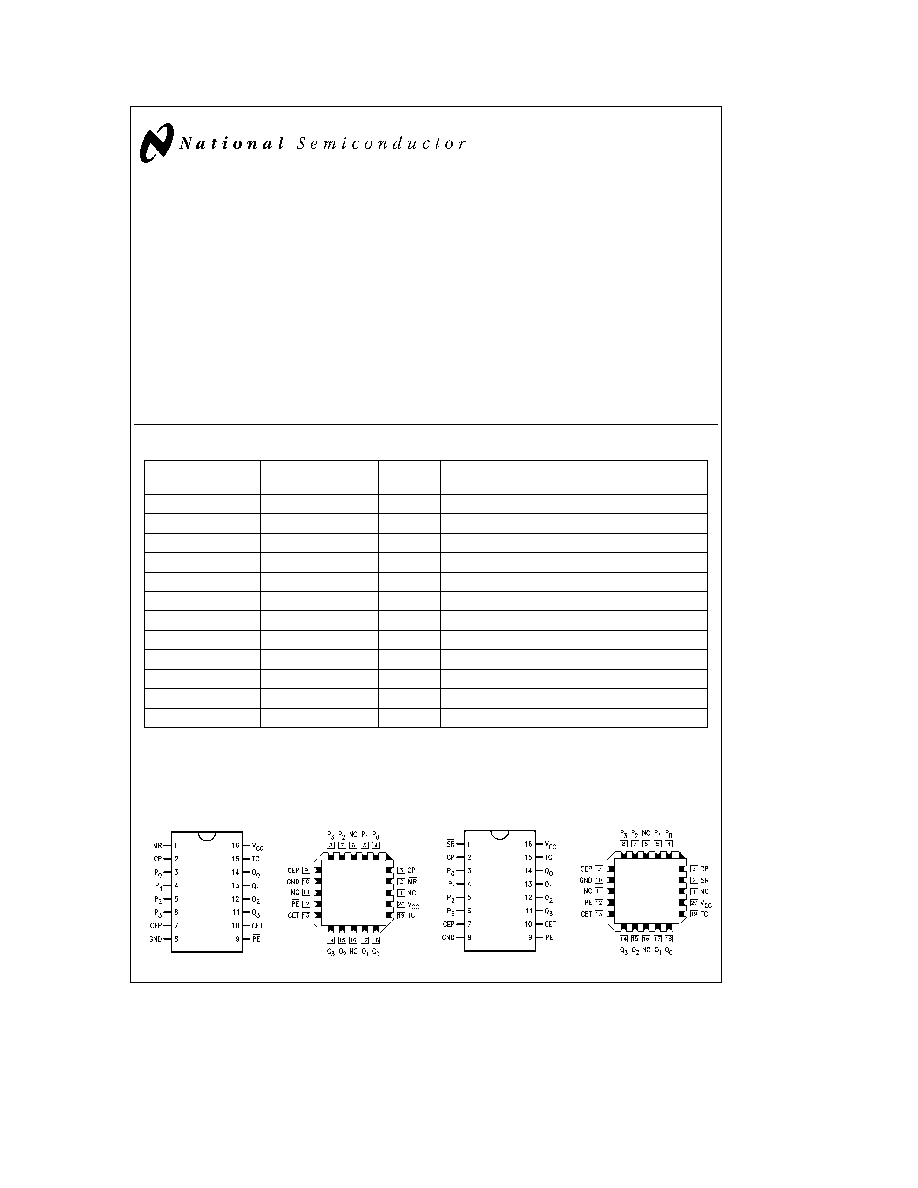
Connection Diagrams
Pin Assignment
for DIP SOIC and Flatpak
'F161A
TL F 9486 ≠ 1
Pin Assignment
for LCC
'F161A
TL F 9486 ≠ 2
Pin Assignment
for DIP SOIC and Flatpak
'F163A
TL F 9486 ≠ 7
Pin Assignment
for LCC
'F163A
TL F 9486 ≠ 8
TRI-STATE
is a registered trademark of National Semiconductor Corporation
C1995 National Semiconductor Corporation
RRD-B30M75 Printed in U S A
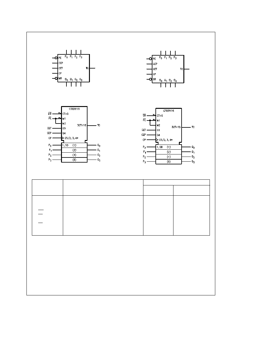
Logic Symbols
'F161A
TL F 9486 ≠ 3
IEEE IEC
'F161A
TL F 9486 ≠ 6
'F163A
TL F 9486 ≠ 9
IEEE IEC
'F163A
TL F 9486 ≠ 10
Unit Loading Fan Out
54F 74F
Pin Names
Description
U L
Input I
IH
I
IL
HIGH LOW
Output I
OH
I
OL
CEP
Count Enable Parallel Input
1 0 1 0
20 mA
b
0 6 mA
CET
Count Enable Trickle Input
1 0 2 0
20 mA
b
1 2 mA
CP
Clock Pulse Input (Active Rising Edge)
1 0 1 0
20 mA
b
0 6 mA
MR ('F161A)
Asynchronous Master Reset Input (Active LOW)
1 0 1 0
20 mA
b
0 6 mA
SR ('F163A)
Synchronous Reset Input (Active LOW)
1 0 2 0
20 mA
b
1 2 mA
P
0
≠ P
3
Parallel Data Inputs
1 0 1 0
20 mA
b
0 6 mA
PE
Parallel Enable Input (Active LOW)
1 0 2 0
20 mA
b
1 2 mA
Q
0
≠ Q
3
Flip-Flop Outputs
50 33 3
b
1 mA 20 mA
TC
Terminal Count Output
50 33 3
b
1 mA 20 mA
2

Functional Description
The 'F161A and 'F163A count in modulo-16 binary se-
quence From state 15 (HHHH) they increment to state 0
(LLLL) The clock inputs of all flip-flops are driven in parallel
through a clock buffer Thus all changes of the Q outputs
(except due to Master Reset of the 'F161A) occur as a re-
sult of and synchronous with the LOW-to-HIGH transition
of the CP input signal The circuits have four fundamental
modes of operation in order of precedence asynchronous
reset ('F161A) synchronous reset ('F163A) parallel load
count-up and hold Five control inputs
Master Reset (MR
'F161A) Synchronous Reset (SR 'F163A) Parallel Enable
(PE) Count Enable Parallel (CEP) and Count Enable Trickle
(CET)
determine the mode of operation as shown in the
Mode Select Table A LOW signal on MR overrides all other
inputs and asynchronously forces all outputs LOW A LOW
signal on SR overrides counting and parallel loading and
allows all outputs to go LOW on the next rising edge of CP
A LOW signal on PE overrides counting and allows informa-
tion on the Parallel Data (P
n
) inputs to be loaded into the
flip-flops on the next rising edge of CP With PE and MR
('F161A) or SR ('F163A) HIGH CEP and CET permit count-
ing when both are HIGH Conversely a LOW signal on ei-
ther CEP or CET inhibits counting
The 'F161A and 'F163A use D-type edge triggered flip-flops
and changing the SR PE CEP and CET inputs when the CP
is in either state does not cause errors provided that the
recommended setup and hold times with respect to the ris-
ing edge of CP are observed
The Terminal Count (TC) output is HIGH when CET is HIGH
and the counter is in state 15 To implement synchronous
multi-stage counters the TC outputs can be used with the
CEP and CET inputs in two different ways Please refer to
the 'F568 data sheet The TC output is subject to decoding
spikes due to internal race conditions and is therefore not
recommended for use as a clock or asynchronous reset for
flip-flops counters or registers
Logic Equations Count Enable
e
CEP
CET
PE
TC
e
Q
0
Q
1
Q
2
Q
3
CET
Mode Select Table
SR
PE
CET
CEP
Action on the Rising
Clock Edge (
L)
L
X
X
X
Reset (Clear)
H
L
X
X
Load (P
n
x
Q
n
)
H
H
H
H
Count (Increment)
H
H
L
X
No Change (Hold)
H
H
X
L
No Change (Hold)
For 'F163A only
H
e
HIGH Voltage Level
L
e
LOW Voltage Level
X
e
Immaterial
State Diagram
TL F 9486 ≠ 5
3
Block Diagram
TLF9486
≠
4
4
Absolute Maximum Ratings
(Note 1)
If Military Aerospace specified devices are required
please contact the National Semiconductor Sales
Office Distributors for availability and specifications
Storage Temperature
b
65 C to
a
150 C
Ambient Temperature under Bias
b
55 C to
a
125 C
Junction Temperature under Bias
b
55 C to
a
175 C
Plastic
b
55 C to
a
150 C
V
CC
Pin Potential to
Ground Pin
b
0 5V to
a
7 0V
Input Voltage (Note 2)
b
0 5V to
a
7 0V
Input Current (Note 2)
b
30 mA to
a
5 0 mA
Voltage Applied to Output
in HIGH State (with V
CC
e
0V)
Standard Output
b
0 5V to V
CC
TRI-STATE Output
b
0 5V to
a
5 5V
Current Applied to Output
in LOW State (Max)
twice the rated I
OL
(mA)
ESD Last Passing Voltage (Min)
4000V
Note 1
Absolute maximum ratings are values beyond which the device may
be damaged or have its useful life impaired Functional operation under
these conditions is not implied
Note 2
Either voltage limit or current limit is sufficient to protect inputs
Recommended Operating
Conditions
Free Air Ambient Temperature
Military
b
55 C to
a
125 C
Commercial
0 C to
a
70 C
Supply Voltage
Military
a
4 5V to
a
5 5V
Commercial
a
4 5V to
a
5 5V
DC Electrical Characteristics
Symbol
Parameter
54F 74F
Units
V
CC
Conditions
Min
Typ
Max
V
IH
Input HIGH Voltage
2 0
V
Recognized as a HIGH Signal
V
IL
Input LOW Voltage
0 8
V
Recognized as a LOW Signal
V
CD
Input Clamp Diode Voltage
b
1 2
V
Min
I
IN
e b
18 mA
V
OH
Output HIGH
54F 10% V
CC
2 5
I
OH
e b
1 mA
Voltage
74F 10% V
CC
2 5
V
Min
74F 5% V
CC
2 7
V
OL
Output LOW
54F 10% V
CC
0 5
V
Min
I
OL
e
20 mA
Voltage
74F 10% V
CC
0 5
I
IH
Input HIGH
54F
20 0
m
A
Max
V
IN
e
2 7V
Current
74F
5 0
I
BVI
Input HIGH Current
54F
100
m
A
Max
V
IN
e
7 0V
Breakdown Test
74F
7 0
I
CEX
Output HIGH
54F
250
m
A
Max
V
OUT
e
V
CC
Leakage Current
74F
50
V
ID
Input Leakage
74F
4 75
V
0 0
I
ID
e
1 9 mA
Test
All Other Pins Grounded
I
OD
Output Leakage
74F
3 75
m
A
0 0
V
IOD
e
150 mV
Circuit Current
All Other Pins Grounded
I
IL
Input LOW Current
b
0 6
mA
Max
V
IN
e
0 5V (CEP CP MR P
0
≠ P
3
)
b
1 2
mA
Max
V
IN
e
0 5V (CET PE SR)
I
OS
Output Short-Circuit Current
b
60
b
150
mA
Max
V
OUT
e
0V
I
CC
Power Supply Current
37
55
mA
Max
5