
TL F 9489
54F74F174
Hex
D
Flip-Flop
with
Master
Reset
November 1994
54F 74F174 Hex D Flip-Flop with Master Reset
General Description
The 'F174 is a high-speed hex D flip-flop The device is
used primarily as a 6-bit edge-triggered storage register
The information on the D inputs is transferred to storage
during the LOW-to-HIGH clock transition The device has a
Master Reset to simultaneously clear all flip-flops
Features
Y
Edge-triggered D-type inputs
Y
Buffered positive edge-triggered clock
Y
Asynchronous common reset
Y
Guaranteed 4000V minimum ESD protection
Commercial
Military
Package
Package Description
Number
74F174PC
N16E
16-Lead (0 300 Wide) Molded Dual-In-Line
54F174DM (Note 2)
J16A
16-Lead Ceramic Dual-In-Line
74F174SC (Note 1)
M16A
16-Lead (0 150 Wide) Molded Small Outline JEDEC
74F174SJ (Note 1)
M16D
16-Lead (0 300 Wide) Molded Small Outline EIAJ
54F174FM (Note 2)
W16A
16-Lead Cerpack
54F174LM (Note 2)
E20A
20-Lead Ceramic Leadless Chip Carrier Type C
Note 1
Devices also available in 13
reel Use Suffix
e
SCX and SJX
Note 2
Military grade device with environmental and burn-in processing Use suffix
e
DMQB FMQB and LMQB
Logic Symbols
Connection Diagrams
TL F 9489 � 3
IEEE IEC
TL F 9489 � 5
Pin Assignment for
DIP SOIC and Flatpak
TL F 9489 � 1
Pin Assignment
for LCC
TL F 9489 � 2
TRI-STATE
is a registered trademark of National Semiconductor Corporation
C1995 National Semiconductor Corporation
RRD-B30M75 Printed in U S A
Unit Loading Fan Out
54F 74F
Pin Names
Description
U L
Input I
IH
I
IL
HIGH LOW
Output I
OH
I
OL
D
0
� D
5
Data Inputs
1 0 1 0
20 mA
b
0 6 mA
CP
Clock Pulse Input (Active Rising Edge)
1 0 1 0
20 mA
b
0 6 mA
MR
Master Reset Input (Active LOW)
1 0 1 0
20 mA
b
0 6 mA
Q
0
� Q
5
Outputs
50 33 3
b
1 mA 20 mA
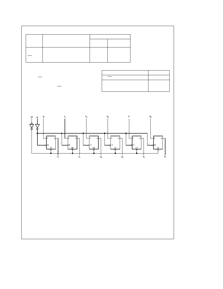
Functional Description
The 'F174 consists of six edge-triggered D flip-flops with
individual D inputs and Q outputs The Clock (CP) and Mas-
ter Reset (MR) are common to all flip-flops Each D input's
state is transferred to the corresponding flip-flop's output
following the LOW-to-HIGH Clock (CP) transition A LOW
input to the Master Reset (MR) will force all outputs LOW
independent of Clock or Data inputs The 'F174 is useful for
applications where the true output only is required and the
Clock and Master Reset are common to all storage ele-
ments
Truth Table
Inputs
Outputs
MR
CP
D
n
Q
n
L
X
X
L
H
L
H
H
H
L
L
L
H
e
HIGH Voltage Level
L
e
LOW Voltage Level
X
e
Immaterial
L
e
LOW-to-HIGH Clock Transition
Logic Diagram
TL F 9489 � 4
Please note that this diagram is provided only for the understanding of logic operations and should not be used to estimate propagation delays
2

Absolute Maximum Ratings
(Note 1)
If Military Aerospace specified devices are required
please contact the National Semiconductor Sales
Office Distributors for availability and specifications
Storage Temperature
b
65 C to
a
150 C
Ambient Temperature under Bias
b
55 C to
a
125 C
Junction Temperature under Bias
b
55 C to
a
175 C
Plastic
b
55 C to
a
150 C
V
CC
Pin Potential to
Ground Pin
b
0 5V to
a
7 0V
Input Voltage (Note 2)
b
0 5V to
a
7 0V
Input Current (Note 2)
b
30 mA to
a
5 0 mA
Voltage Applied to Output
in HIGH State (with V
CC
e
0V)
Standard Output
b
0 5V to V
CC
TRI-STATE Output
b
0 5V to
a
5 5V
Current Applied to Output
in LOW State (Max)
twice the rated I
OL
(mA)
ESD Last Passing Voltage (Min)
4000V
Note 1
Absolute maximum ratings are values beyond which the device may
be damaged or have its useful life impaired Functional operation under
these conditions is not implied
Note 2
Either voltage limit or current limit is sufficient to protect inputs
Recommended Operating
Conditions
Free Air Ambient Temperature
Military
b
55 C to
a
125 C
Commercial
0 C to
a
70 C
Supply Voltage
Military
a
4 5V to
a
5 5V
Commercial
a
4 5V to
a
5 5V
DC Electrical Characteristics
Symbol
Parameter
54F 74F
Units
V
CC
Conditions
Min
Typ
Max
V
IH
Input HIGH Voltage
2 0
V
Recognized as a HIGH Signal
V
IL
Input LOW Voltage
0 8
V
Recognized as a LOW Signal
V
CD
Input Clamp Diode Voltage
b
1 2
V
Min
I
IN
e b
18 mA
V
OH
Output HIGH
54F 10% V
CC
2 5
I
OH
e b
1 mA
Voltage
74F 10% V
CC
2 5
V
Min
I
OH
e b
1 mA
74F 5% V
CC
2 7
I
OH
e b
1 mA
V
OL
Output LOW
54F 10% V
CC
0 5
V
Min
I
OL
e
20 mA
Voltage
74F 10% V
CC
0 5
I
OL
e
20 mA
I
IH
Input HIGH
54F
20 0
m
A
Max
V
IN
e
2 7V
Current
74F
5 0
I
BVI
Input HIGH Current
54F
100
m
A
Max
V
IN
e
7 0V
Breakdown Test
74F
7 0
I
CEX
Output HIGH
54F
250
m
A
Max
V
OUT
e
V
CC
Leakage Current
74F
50
V
ID
Input Leakage
74F
4 75
V
0 0
I
ID
e
1 9 mA
Test
All Other Pins Grounded
I
OD
Output Leakage
74F
3 75
m
A
0 0
V
IOD
e
150 mV
Circuit Current
All Other Pins Grounded
I
IL
Input LOW Current
b
0 6
mA
Max
V
IN
e
0 5V
I
OS
Output Short-Circuit Current
b
60
b
150
mA
Max
V
OUT
e
0V
I
CCH
Power Supply Current
30
45
mA
Max
CP
e
L
D
n
e
MR
e
HIGH
I
CCL
Power Supply Current
30
45
mA
Max
V
O
e
LOW
3

AC Electrical Characteristics
74F
54F
74F
T
A
e a
25 C
T
A
V
CC
e
Mil
T
A
V
CC
e
Com
Symbol
Parameter
V
CC
e a
5 0V
C
L
e
50 pF
C
L
e
50 pF
Units
C
L
e
50 pF
Min
Typ
Max
Min
Max
Min
Max
f
max
Maximum Clock Frequency
80
70
80
MHz
t
PLH
Propagation Delay
3 5
5 5
8 0
3 0
10 0
3 5
9 0
ns
t
PHL
CP to Q
n
4 0
7 0
10 0
4 0
12 0
4 0
11 0
t
PHL
Propagation Delay
5 0
10 0
14 0
5 0
16 0
5 0
15 0
ns
MR to Q
n
AC Operating Requirements
74F
54F
74F
Symbol
Parameter
T
A
e a
25 C
T
A
V
CC
e
Mil
T
A
V
CC
e
Com
Units
V
CC
e a
5 0V
Min
Max
Min
Max
Min
Max
t
s
(H)
Setup Time HIGH or LOW
4 8
5 0
4 8
t
s
(L)
D
n
to CP
4 0
5 0
4 0
ns
t
h
(H)
Hold Time HIGH or LOW
0
2 0
0
t
h
(L)
D
n
to CP
0
2 0
0
t
w
(H)
CP Pulse Width
4 0
5 0
4 0
ns
t
w
(L)
HIGH or LOW
6 0
7 5
6 0
t
w
(L)
MR Pulse Width LOW
5 0
6 5
5 0
ns
t
rec
Recovery Time MR to CP
5 0
6 0
5 0
4
Ordering Information
The device number is used to form part of a simplified purchasing code where the package type and temperature range are
defined as follows
74F
174
S
C
X
Temperature Range Family
Special Variations
74F
e
Commercial
QB
e
Military grade device with
54F
e
Military
environmental and burn-in
processing
Device Type
X
e
Devices shipped in 13 reel
Package Code
Temperature Range
P
e
Plastic DIP
C
e
Commercial (0 C to
a
70 C)
D
e
Ceramic DIP
M
e
Military (
b
55 C to
a
125 C)
F
e
Flatpak
L
e
Leadless Chip Carrier (LCC)
S
e
Small Outline SOIC JEDEC
SS
e
Small Outline SOIC EIAJ
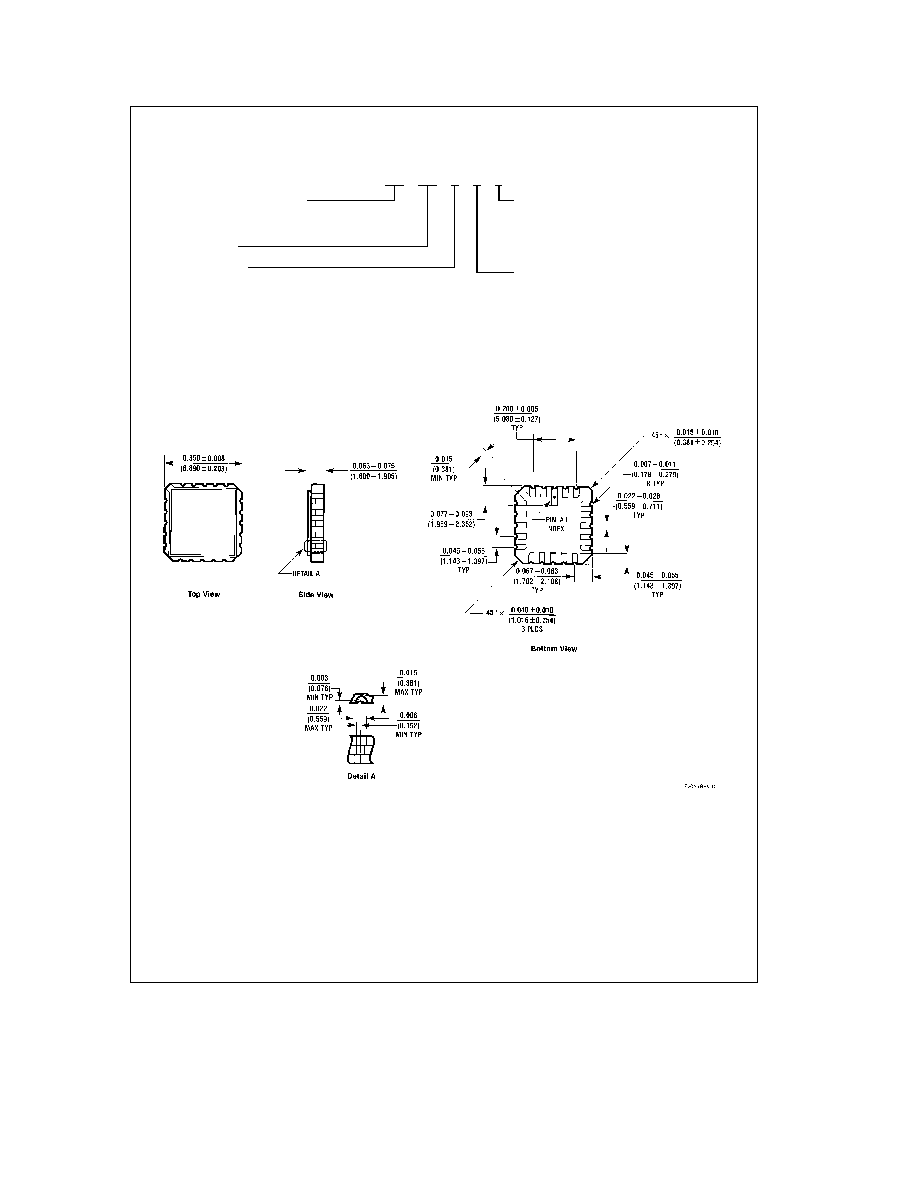
Physical Dimensions
inches (millimeters)
20-Terminal Ceramic Leadless Chip Carrier (L)
NS Package Number E20A
5