
TL F 9533
54F74F398
54F74F399
Quad
2-Port
Register
May 1995
54F 74F398
54F 74F399
Quad 2-Port Register
General Description
The 'F398 and 'F399 are the logical equivalents of a quad
2-input multiplexer feeding into four edge-triggered flip-
flops A common Select input determines which of the two
4-bit words is accepted The selected data enters the flip-
flops on the rising edge of the clock The 'F399 is the 16-pin
version of the 'F398 with only the Q outputs of the flip-flops
available
Features
Y
Select inputs from two data sources
Y
Fully positive edge-triggered operation
Y
Both true and complement outputs
'F398
Y
Guaranteed 4000V minimum ESD protection
'F399
Commercial
Military
Package
Package Description
Number
74F398PC
N20A
20-Lead (0 300 Wide) Molded Dual-In-Line
54F398DM (Note 2)
J20A
20-Lead Ceramic Dual-In-Line
74F398SC (Note 1)
M20B
20-Lead (0 300 Wide) Molded Small Outline JEDEC
54F398FM (Note 2)
W20A
20-Lead Cerpack
54F398LM (Note 2)
E20A
20-Lead Ceramic Leadless Chip Carrier Type C
74F399PC
N20A
20-Lead (0 300 Wide) Molded Dual-In-Line
54F399DM (Note 2)
J20A
20-Lead Ceramic Dual-In-Line
74F399SC (Note 1)
M20B
20-Lead (0 300 Wide) Molded Small Outline JEDEC
74F399SJ (Note 1)
M20D
20-Lead (0 300 Wide) Molded Small Outline EIAJ
54F399FM (Note 2)
W20A
20-Lead Cerpack
54F399LM (Note 2)
E20A
20-Lead Ceramic Leadless Chip Carrier Type C
Note 1
Devices also available in 13
reel Use suffix
e
SCX and SJX
Note 2
Military grade device with environmental and burn-in processing Use suffix
e
DMQB FMQB and LMQB
Connection Diagrams
'F398
Pin Assignment
for LCC
TL F 9533 � 5
Pin Assignment
for DIP SOIC and Flatpak
TL F 9533 � 6
TRI-STATE
is a registered trademark of National Semiconductor Corporation
C1995 National Semiconductor Corporation
RRD-B30M75 Printed in U S A
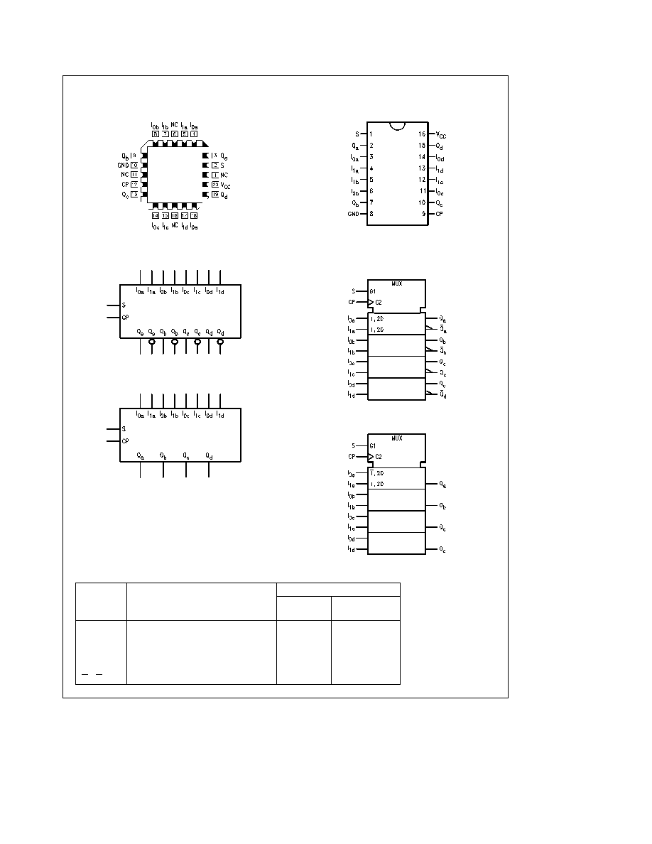
Connection Diagrams
(Continued)
'F399
TL F 9533 � 7
TL F 9533 � 8
Logic Symbols
'F398
TL F 9533 � 2
'F399
TL F 9533 � 4
IEEE IEC
'F398
TL F 9533 � 1
'F399
TL F 9533 � 3
Unit Loading Fan Out
54F 74F
Pin Names
Description
U L
Input I
IH
I
IL
HIGH LOW
Output I
OH
I
OL
S
Common Select Input
1 0 1 0
20 mA
b
0 6 mA
CP
Clock Pulse Input (Active Rising Edge)
1 0 1 0
20 mA
b
0 6 mA
I
0a
� I
0d
Data Inputs from Source 0
1 0 1 0
20 mA
b
0 6 mA
I
1a
� I
1d
Data Inputs from Source 1
1 0 1 0
20 mA
b
0 6 mA
Q
a
� Q
d
Register True Outputs
50 33 3
b
1 mA 20 mA
Q
a
� Q
d
Register Complementary Outputs ('F398)
50 33 3
b
1 mA 20 mA
2

Functional Description
The 'F398 and 'F399 are high-speed quad 2-port registers
They select four bits of data from either of two sources
(Ports) under control of a common Select input (S) The
selected data is transferred to a 4-bit output register syn-
chronous with the LOW-to-HIGH transition of the Clock in-
put (CP) The 4-bit D-type output register is fully edge-trig-
gered The Data inputs (I
0x
I
1x
) and Select input (S) must be
stable only a setup time prior to and hold time after the
LOW-to-HIGH transition of the Clock input for predictable
operation The 'F398 has both Q and Q outputs
Function Table
Inputs
Outputs
S
I
0
I
1
Q
Q
I
I
X
L
H
I
h
X
H
L
h
X
I
L
H
h
X
h
H
L
H
e
HIGH Voltage Level
L
e
LOW Voltage Level
h
e
HIGH Voltage Level one setup time prior to the LOW-to-HIGH clock
transition
I
e
LOW Voltage Level one setup time prior to the LOW-to-HIGH clock
transition
X
e
Immaterial
'F398 only
Logic Diagram
TL F 9533 � 9
'F398 Only
Please note that this diagram is provided only for the understanding of logic operations and should not be used to estimate propagation delays
3

Absolute Maximum Ratings
(Note 1)
If Military Aerospace specified devices are required
please contact the National Semiconductor Sales
Office Distributors for availability and specifications
Storage Temperature
b
65 C to
a
150 C
Ambient Temperature under Bias
b
55 C to
a
125 C
Junction Temperature under Bias
b
55 C to
a
175 C
Plastic
b
55 C to
a
150 C
V
CC
Pin Potential to
Ground Pin
b
0 5V to
a
7 0V
Input Voltage (Note 2)
b
0 5V to
a
7 0V
Input Current (Note 2)
b
30 mA to
a
5 0 mA
Voltage Applied to Output
in HIGH State (with V
CC
e
0V)
Standard Output
b
0 5V to V
CC
TRI-STATE Output
b
0 5V to
a
5 5V
Current Applied to Output
in LOW State (Max)
twice the rated I
OL
(mA)
ESD Last Passing Voltage (Min)
'F399
4000V
Note 1
Absolute maximum ratings are values beyond which the device may
be damaged or have its useful life impaired Functional operation under
these conditions is not implied
Note 2
Either voltage limit or current limit is sufficient to protect inputs
Recommended Operating
Conditions
Free Air Ambient Temperature
Military
b
55 C to
a
125 C
Commercial
0 C to
a
70 C
Supply Voltage
Military
a
4 5V to
a
5 5V
Commercial
a
4 5V to
a
5 5V
DC Electrical Characteristics
Symbol
Parameter
54F 74F
Units
V
CC
Conditions
Min
Typ
Max
V
IH
Input HIGH Voltage
2 0
V
Recognized as a HIGH Signal
V
IL
Input LOW Voltage
0 8
V
Recognized as a LOW Signal
V
CD
Input Clamp Diode Voltage
b
1 2
V
Min
I
IN
e b
18 mA
V
OH
Output HIGH
54F 10% V
CC
2 5
I
OH
e b
1 mA
Voltage
74F 10% V
CC
2 5
V
Min
I
OH
e b
1 mA
74F 5% V
CC
2 7
I
OH
e b
1 mA
V
OL
Output LOW
54F 10% V
CC
0 5
V
Min
I
OL
e
20 mA
Voltage
74F 10% V
CC
0 5
I
OL
e
20 mA
I
IH
Input HIGH Current
54F
20 0
m
A
Max
V
IN
e
2 7V
74F
5 0
I
BVI
Input HIGH Current
54F
100
m
A
Max
V
IN
e
7 0V
Breakdown Test
74F
7 0
I
CEX
Output HIGH
54F
250
m
A
Max
V
OUT
e
V
CC
Leakage Current
74F
50
V
ID
Input Leakage
74F
4 75
V
0 0
I
ID
e
1 9 mA
Test
All Other Pins Grounded
I
OD
Output Leakage
74F
3 75
m
A
0 0
V
IOD
e
150 mV
Circuit Current
All Other Pins Grounded
I
IL
Input LOW Current
b
0 6
mA
Max
V
IN
e
0 5V
I
OS
Output Short-Circuit Current
b
60
b
150
mA
Max
V
OUT
e
0V
I
CCH
Power Supply Current ('F398)
25
38
mA
Max
V
O
e
HIGH
I
CCL
Power Supply Current ('F398)
25
38
mA
Max
V
O
e
LOW
I
CCH
Power Supply Current ('F399)
22
34
mA
Max
V
O
e
HIGH
I
CCL
Power Supply Current ('F399)
22
34
mA
Max
V
O
e
LOW
4
AC Electrical Characteristics
74F
54F
74F
T
A
e a
25 C
T
A
V
CC
e
Mil
T
A
V
CC
e
Com
Symbol
Parameter
V
CC
e a
5 0V
C
L
e
50 pF
C
L
e
50 pF
Units
C
L
e
50 pF
Min
Typ
Max
Min
Max
Min
Max
f
max
Input Clock Frequency
100
140
80
100
MHz
t
PLH
Propagation Delay
3 0
5 7
7 5
3 0
9 5
3 0
8 5
ns
t
PHL
CP to Q or Q
3 0
6 8
9 0
3 0
11 5
3 0
10 0
'F398 3 3 ns
AC Operating Requirements
74F
54F
74F
Symbol
Parameter
T
A
e a
25 C
T
A
V
CC
e
Mil
T
A
V
CC
e
Com
Units
V
CC
e a
5 0V
Min
Max
Min
Max
Min
Max
t
s
(H)
Setup Time HIGH or LOW
3 0
4 5
3 0
t
s
(L)
I
n
to CP
3 0
4 5
3 0
ns
t
h
(H)
Hold Time HIGH or LOW
1 0
1 5
1 0
t
h
(L)
I
n
to CP
1 0
1 5
1 0
t
s
(H)
Setup Time HIGH or LOW
7 5
10 5
8 5
t
s
(L)
S to CP ('F398)
7 5
10 5
8 5
t
s
(H)
Setup Time HIGH or LOW
7 5
9 5
8 5
ns
t
s
(L)
S to CP ('F399)
7 5
9 5
8 5
t
h
(H)
Hold Time HIGH or LOW
0
0
0
t
h
(L)
S to CP
0
0
0
t
w
(H)
CP Pulse Width
4 0
4 0
4 0
ns
t
w
(L)
HIGH or LOW
5 0
7 0
5 0
5