TL F 9537
54F407
Data
Access
Register
December 1994
54F407
Data Access Register
General Description
The 'F407 Data Access Register (DAR) performs memory
address arithmetic for RAM resident stack applications It
contains three 4-bit registers intended for Program Counter
(R
0
) Stack Pointer (R
1
) and Operand Address (R
2
) The
'F407 implements 16 instructions which allow either pre- or
post-decrement increment and register-to-register transfer
in a single clock cycle It is expandable in 4-bit increments
and can operate at a 30 MHz microinstruction rate on a
16-bit word The TRI-STATE
outputs are provided for bus-
oriented applications The 'F407 is fully compatible with all
TTL families
Features
Y
High-speed
greater than a 30 MHz microinstruction
rate
Y
Three 4-bit registers
Y
16 instructions for register manipulation
Y
Two separate output ports one transparent
Y
Relative addressing capability
Y
TRI-STATE Outputs
Y
Optional pre- or post- arithmetic
Y
Expandable in multiples of four bits
Y
24-pin slim package
Y
9407 replacement
Military
Package
Package Description
Number
54F407DM (Note 1)
J24A
24-Lead Ceramic Dual-In-Line
54F407SDM (Note 1)
J24F
24-Lead (0 300 Wide) Ceramic Dual-In-Line
54F407FM (Note 1)
W24C
24-Lead Cerpack
54F407FM (Note 1)
E28A
28-Lead Ceramic Leadless Chip Carrier Type C
Note 1
Military grade device with environmental and burn-in processing Use suffix
e
DMQB FMQB and LMQB
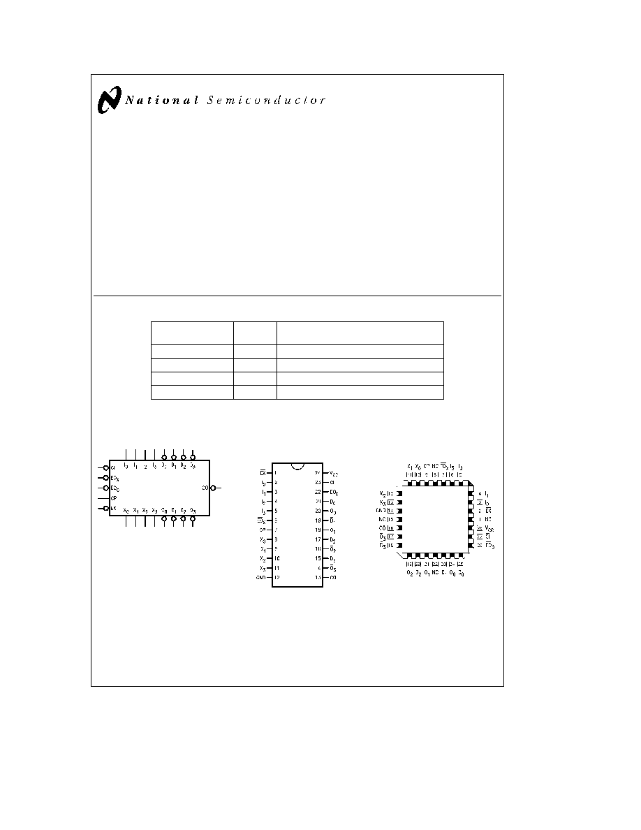
Logic Symbol
Connection Diagrams
TL F 9537 ≠ 3
Pin Assignment
for DIP and Flatpak
TL F 9537 ≠ 1
Pin Assignment
for LCC
TL F 9537 ≠ 2
TRI-STATE
is a registered trademark of National Semiconductor Corporation
C1995 National Semiconductor Corporation
RRD-B30M105 Printed in U S A

Unit Loading Fan Out
54F
Pin Names
Description
U L
Input I
IH
I
IL
HIGH LOW
Output I
OH
I
OL
D
0
≠ D
3
Data Inputs (Active LOW)
1 0 0 67
20 mA
b
0 4 mA
I
0
≠ I
3
Instruction Word Inputs
1 0 0 67
20 mA
b
0 4 mA
CI
Carry Input (Active LOW)
1 0 0 67
20 mA
b
0 4 mA
CO
Carry Output (Active LOW)
20 13 3 (0 67)
0 4 mA 8 mA (4 mA)
CP
Clock Input (L-H Edge-Triggered)
1 0 0 67
20 mA
b
0 4 mA
EX
Execute Input (Active LOW)
1 0 0 67
20 mA
b
0 4 mA
EO
X
Address Output Enable Input (Active LOW)
1 0 0 67
20 mA
b
0 4 mA
EO
0
Data Output Enable Input (Active LOW)
1 0 0 67
20 mA
b
0 4 mA
X
0
≠ X
3
Address Outputs
284 (100) 26 7 (13 3)
b
5 7 mA (2 mA) 16 mA (8 mA)
O
0
≠ O
3
Data Outputs (Active LOW)
284 (100) 26 7 (13 3)
b
5 7 mA (2 mA) 16 mA (8 mA)
Functional Description
The 'F407 contains a 4-bit slice of three Registers (R
0
≠ R
2
)
a 4-bit Adder a TRI-STATE Address Output Buffer (X
0
≠ X
3
)
and a separate Output Register with TRI-STATE buffers
(O
0
≠ O
3
) allowing output of the register contents on the
data bus (refer to the Block Diagram) The DAR performs
sixteen instructions selected by I
0
≠ I
3
as listed in the Func-
tion Table
The 'F407 operates on a single clock CP and EX are inputs
to a 2-input active LOW AND gate For normal operation EX
is brought LOW while CP is HIGH A microcycle starts as the
clock goes HIGH Data inputs D
0
≠ D
3
are applied to the
Adder as one of the operands Three of the four instruction
lines (I
1
≠ I
2
≠ I
3
) select which of the three registers if any is
to be used as the other operand The LOW-to-HIGH CP
transition writes the result from the Adder into a register
(R
0
≠ R
2
) and into the output register provided EX is LOW If
the I
0
instruction input is HIGH the multiplexer routes the
result from the Adder to the TRI-STATE Buffer controlling
the address bus (X
0
≠ X
3
) independent of EX and CP The
'F407 is organized as a 4-bit register slice The active LOW
CI and CO lines allow ripple-carry expansion over longer
word lengths
In a typical application the register utilization in the DAR
may be as follows R
0
is the Program Counter (PC) R
1
is
the Stack Pointer (SP) for memory resident stacks and R
2
contains the operand address For an instruction Fetch PC
can be gated on the X-Bus while it is being incremented
(i e D-Bus
e
1) If the fetched instruction calls for an effec-
tive address for execution which is displaced from the PC
the displacement can be added to the PC and loaded into
R
2
during the next microcycle
Function Table
Instruction
Combinatorial Function
Sequential Function Occurring
I
3
I
2
I
1
I
0
Available on the X-Bus
on the Next Rising CP Edge
L
L
L
L
R
0
R
0
Plus D Plus CI
x
R
0
and 0-Register
L
L
L
H
R
0
Plus D Plus CI
L
L
H
L
R
0
R
0
Plus D Plus CI
x
R
1
and 0-Register
L
L
H
H
R
0
Plus D Plus CI
L
H
L
L
R
0
R
0
Plus D Plus CI
x
R
2
and 0-Register
L
H
L
H
R
0
Plus D Plus CI
L
H
H
L
R
1
R
1
Plus D Plus CI
x
R
1
and 0-Register
L
H
H
H
R
1
Plus D Plus CI
H
L
L
L
R
2
D Plus CI
x
R
2
and 0-Register
H
L
L
H
D Plus CI
H
L
H
L
R
0
D Plus CI
x
R
0
and 0-Register
H
L
H
H
D Plus CI
H
H
L
L
R
2
R
2
Plus D Plus CI
x
R
2
and 0-Register
H
H
L
H
R
2
Plus D Plus CI
H
H
H
L
R
1
D Plus CI
x
R
1
and 0-Register
H
H
H
H
D Plus CI
H
e
HIGH Voltage Level
L
e
LOW Voltage Level
2

Absolute Maximum Ratings
(Note 1)
If Military Aerospace specified devices are required
please contact the National Semiconductor Sales
Office Distributors for availability and specifications
Storage Temperature
b
65 C to
a
150 C
Ambient Temperature under Bias
b
55 C to
a
125 C
Junction Temperature under Bias
b
55 C to
a
175 C
V
CC
Pin Potential to
Ground Pin
b
0 5V to
a
7 0V
Input Voltage (Note 2)
b
0 5V to
a
7 0V
Input Current (Note 2)
b
30 mA to
a
5 0 mA
Voltage Applied to Output
in HIGH State (with V
CC
e
0V)
Standard Output
b
0 5V to V
CC
TRI-STATE Output
b
0 5V to
a
5 5V
Current Applied to Output
in LOW State (Max)
twice the rated I
OL
(mA)
Note 1
Absolute maximum ratings are values beyond which the device may
be damaged or have its useful life impaired Functional operation under
these conditions is not implied
Note 2
Either voltage limit or current limit is sufficient to protect inputs
Recommended Operating
Conditions
Free Air Ambient Temperature
Military
b
55 C to
a
125 C
Supply Voltage
Military
a
4 5V to
a
5 5V
DC Electrical Characteristics
Symbol
Parameter
54F
Units
V
CC
Conditions
Min
Typ
Max
V
IH
Input HIGH Voltage
2 0
V
Recognized as a HIGH Signal
V
IL
Input LOW Voltage
0 8
V
Recognized as a LOW Signal
V
CD
Input Clamp Diode Voltage
b
1 5
V
Min
I
IN
e b
18 mA
V
OH
Output HIGH
54F 10% V
CC
2 4
V
Min
I
OH
e b
0 4 mA (CO)
Voltage
54F 10% V
CC
2 4
I
OH
e b
2 mA (X
0
≠ X
3
O
0
≠ O
3
)
V
OL
Output LOW
54F 10% V
CC
0 5
V
Min
I
OL
e
4 mA (CO)
Voltage
54F 10% V
CC
0 5
I
OL
e
8 mA (X
0
≠ X
3
O
0
≠ O
3
)
I
IH
Input HIGH Current
54F
20 0
m
A
Max
V
IN
e
2 7V
I
BVI
Input HIGH Current
54F
100
m
A
Max
V
IN
e
7 0V
Breakdown Test
I
CEX
Output HIGH
54F
250
m
A
Max
V
OUT
e
V
CC
Leakage Current
I
IL
Input LOW Current
b
0 4
mA
Max
V
IN
e
0 5V
I
OZH
Output Leakage Current
50
m
A
Max
V
OUT
e
2 7V (X
0
≠ X
3
O
0
≠ O
3
)
I
OZL
Output Leakage Current
b
50
m
A
Max
V
OUT
e
0 5V (X
0
≠ X
3
O
0
≠ O
3
)
I
OS
Output Short-Circuit Current
b
30
b
100
mA
Max
V
OUT
e
0V
I
CC
Power Supply Current
90
145
mA
Max
5

