TL F 9555
54F74F544
Octal
Registered
Transceiver
December 1994
54F 74F544
Octal Registered Transceiver
General Description
The 'F544 octal transceiver contains two sets of D-type
latches for temporary storage of data flowing in either direc-
tion Separate Latch Enable and Output Enable inputs are
provided for each register to permit independent control of
inputting and outputting in either direction of data flow The
A outputs are guaranteed to sink 24 mA (20 mA Mil) while
the B outputs are rated for 64 mA (48 mA Mil) The 'F544
inverts data in both directions
Features
Y
8-bit octal transceiver
Y
Back-to-back registers for storage
Y
Separate controls for data flow in each direction
Y
A outputs sink 24 mA (20 mA Mil) B outputs sink
64 mA (48 mA Mil)
Y
300 mil slim PDIP
Commercial
Military
Package
Package Description
Number
74F544SPC
N24C
24-Lead (0 300 Wide) Molded Dual-In-Line
54F544DM (Note 2)
J24A
24-Lead Ceramic Dual-In-Line
54F544SDM (Note 2)
J24F
24-Lead (0 300 Wide) Ceramic Dual-In-Line
74F544SC (Note 1)
M24B
24-Lead (0 300 Wide) Molded Small Outline JEDEC
74F544MSA (Note 1)
MSA24
24-Lead Molded Shrink Small Outline EIAJ Type II
54F544FM (Note 2)
W24C
24-Lead Cerpack
54F544LM (Note 2)
E28A
24-Lead Ceramic Leadless Chip Carrier Type C
Note 1
Devices also available in 13
reel Use suffix
e
SCX and MSAX
Note 2
Military grade device with environmental and burn-in processing Use suffix
e
DMQB FMQB and LMQB
Logic Symbols
TL F 9555 � 2
IEEE IEC
TL F 9555 � 1
TRI-STATE
is a registered trademark of National Semiconductor Corporation
C1995 National Semiconductor Corporation
RRD-B30M75 Printed in U S A

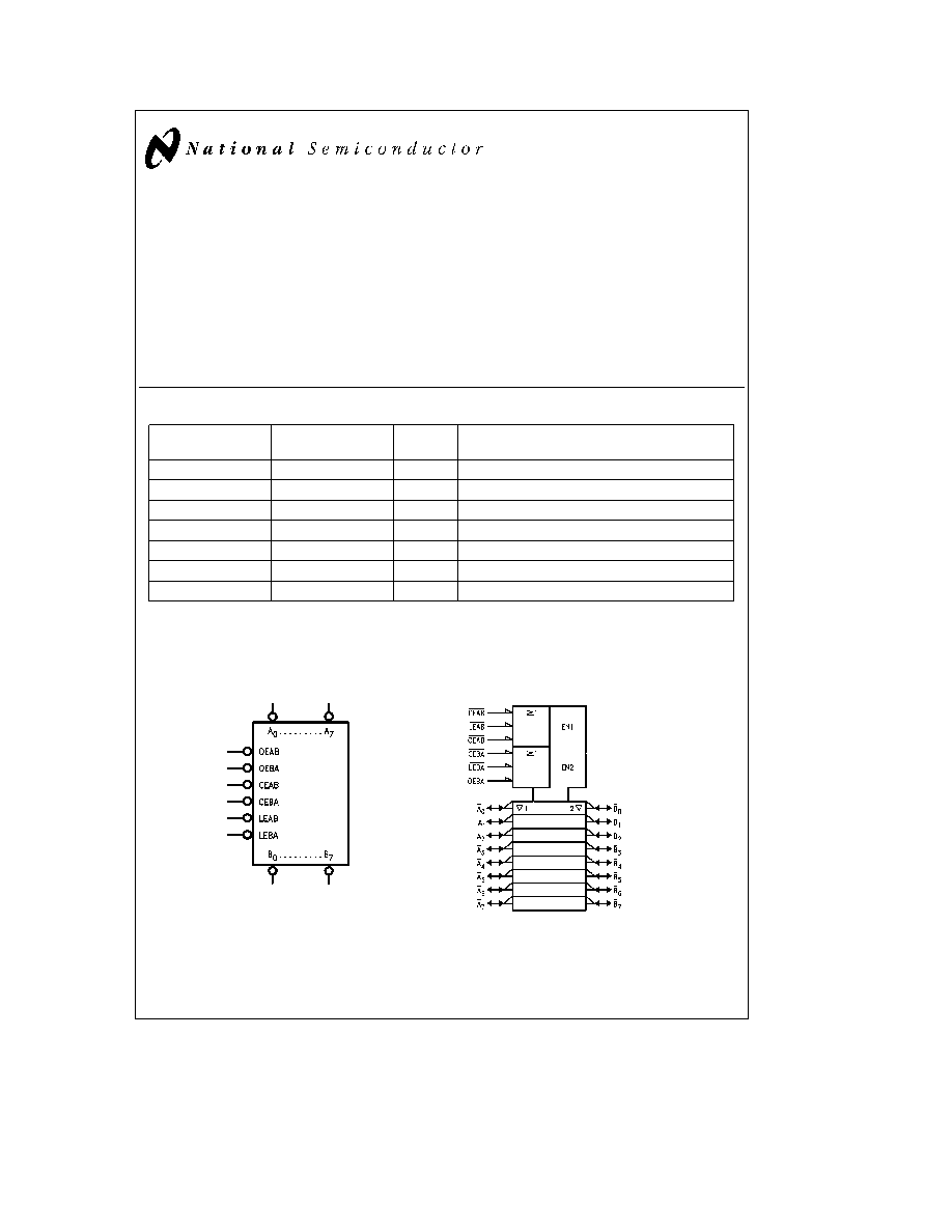
Connection Diagrams
Pin Assignment for
DIP SOIC and Flatpak
TL F 9555 � 3
Pin Assignment
for LCC
TL F 9555 � 4
Unit Loading Fan Out
54F 74F
Pin Names
Description
U L
Input I
IH
I
IL
HIGH LOW
Output I
OH
I
OL
OEAB
A-to-B Output Enable Input (Active LOW)
1 0 1 0
20 mA
b
0 6 mA
OEBA
B-to-A Output Enable Input (Active LOW)
1 0 1 0
20 mA
b
0 6 mA
CEAB
A-to-B Enable Input (Active LOW)
1 0 2 0
20 mA
b
1 2 mA
CEBA
B-to-A Enable Input (Active LOW)
1 0 2 0
20 mA
b
1 2 mA
LEAB
A-to-B Latch Enable Input (Active LOW)
1 0 1 0
20 mA
b
0 6 mA
LEBA
B-to-A Latch Enable Input (Active LOW)
1 0 1 0
20 mA
b
0 6 mA
A
0
� A
7
A-to-B Data Inputs or
3 5 1 083
70 mA
b
650 mA
B-to-A TRI-STATE Outputs
150 40(33 3)
b
3 mA 24 mA (20 mA)
B
0
� B
7
B-to-A Data Inputs or
3 5 1 083
70 mA
b
650 mA
A-to-B TRI-STATE Outputs
600 106 6(80)
b
12 mA 64 mA (48 mA)
Functional Description
The 'F544 contains two sets of eight D-type latches with
separate input and output controls for each set For data
flow from A to B for example the A-to-B Enable (CEAB)
input must be LOW in order to enter data from A
0
� A
7
or
take data from B
0
� B
7
as indicated in the Data I O Control
Table With CEAB LOW a LOW signal on the A-to-B Latch
Enable (LEAB) input makes the A-to-B latches transparent
a subsequent LOW-to-HIGH transition of the LEAB signal
puts the A latches in the storage mode and their outputs no
longer change with the A inputs With CEAB and OEAB both
LOW the TRI-STATE
B output buffers are active and re-
flect the data present at the output of the A latches Control
of data flow from B to A is similar but using the CEBA
LEBA and OEBA inputs
Data I O Control Table
Inputs
Latch Status
Output Buffers
CEAB
LEAB
OEAB
H
X
X
Latched
High Z
X
H
X
Latched
L
L
X
Transparent
X
X
H
High Z
L
X
L
Driving
H
e
HIGH Voltage Level
L
e
LOW Voltage Level
X
e
Immaterial
A-to-B data flow shown B-to-A flow control is the same
except using CEBA LEBA and OEBA
2
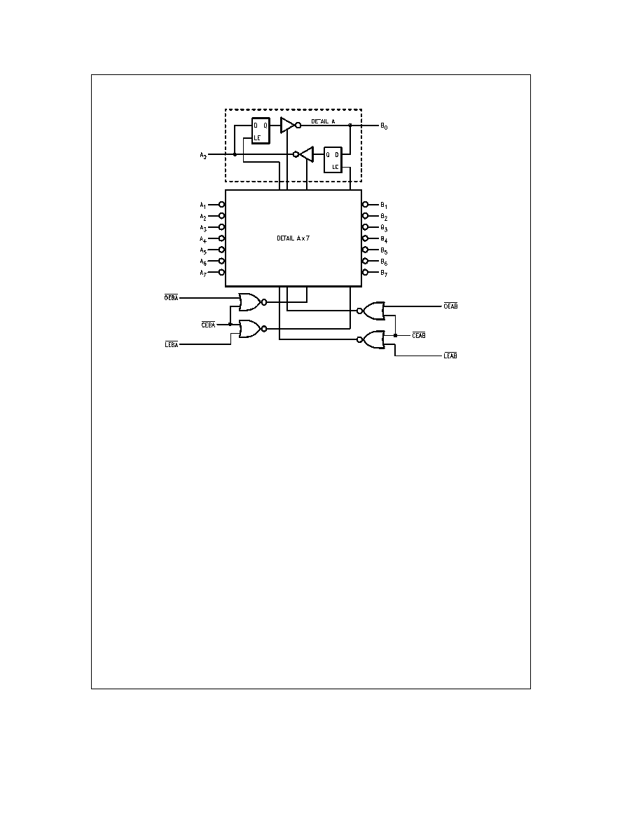
Logic Diagram
TL F 9555 � 5
Please note that this diagram is provided only for the understanding of logic operations and should not be used to estimate propagation delays
3

Absolute Maximum Ratings
(Note 1)
If Military Aerospace specified devices are required
please contact the National Semiconductor Sales
Office Distributors for availability and specifications
Storage Temperature
b
65 C to
a
150 C
Ambient Temperature under Bias
b
55 C to
a
125 C
Junction Temperature under Bias
b
55 C to
a
175 C
Plastic
b
55 C to
a
150 C
V
CC
Pin Potential to
Ground Pin
b
0 5V to
a
7 0V
Input Voltage (Note 2)
b
0 5V to
a
7 0V
Input Current (Note 2)
b
30 mA to
a
5 0 mA
Note 1
Absolute maximum ratings are values beyond which the device may
be damaged or have its useful life impaired Functional operation under
these conditions is not implied
Note 2
Either voltage limit or current limit is sufficient to protect inputs
Voltage Applied to Output
in HIGH State (with V
CC
e
0V)
Standard Output
b
0 5V to V
CC
TRI-STATE Output
b
0 5V to
a
5 5V
Current Applied to Output
in LOW State (Max)
twice the rated I
OL
(mA)
Recommended Operating
Conditions
Free Air Ambient Temperature
Military
b
55 C to
a
125 C
Commercial
0 C to
a
70 C
Supply Voltage
Military
a
4 5V to
a
5 5V
Commercial
a
4 5V to
a
5 5V
DC Electrical Characteristics
Symbol
Parameter
54F 74F
Units
V
CC
Conditions
Min
Typ
Max
V
IH
Input HIGH Voltage
2 0
V
Recognized as a HIGH Signal
V
IL
Input LOW Voltage
0 8
V
Recognized as a LOW Signal
V
CD
Input Clamp Diode Voltage
b
1 2
V
Min
I
IN
e b
18 mA
(except A
n
B
n
)
V
OH
Output HIGH
54F 10% V
CC
2 5
I
OH
e b
1 mA (A
n
)
Voltage
54F 10% V
CC
2 4
I
OH
e b
3 mA (A
n
B
n
)
54F 10% V
CC
2 0
I
OH
e b
12 mA (B
n
)
74F 10% V
CC
2 5
V
Min
I
OH
e b
1 mA (A
n
)
74F 10% V
CC
2 4
I
OH
e b
3 mA (A
n
B
n
)
74F 10% V
CC
2 0
I
OH
e b
15 mA (B
n
)
74F 5% V
CC
2 7
I
OH
e b
1 mA (A
n
)
74F 5% V
CC
2 7
I
OH
e b
3 mA (A
n
B
n
)
V
OL
Output LOW
54F 10% V
CC
0 5
I
OL
e
20 mA (A
n
)
Voltage
54F 10% V
CC
0 55
V
Min
I
OL
e
48 mA (B
n
)
74F 10% V
CC
0 5
I
OL
e
24 mA (A
n
)
74F 10% V
CC
0 55
I
OL
e
64 mA (B
n
)
I
IH
Input HIGH
54F
20 0
m
A
Max
V
IN
e
2 7V (except A
n
B
n
)
Current
74F
5 0
I
BVI
Input HIGH Current
54F
100
m
A
Max
V
IN
e
7 0V (except A
n
B
n
)
Breakdown Test
74F
7 0
I
BVIT
Input HIGH Current
54F
1 0
mA
Max
V
IN
e
5 5V (A
n
B
n
)
Breakdown (I O)
74F
0 5
I
CEX
Output HIGH
54F
250
m
A
Max
V
OUT
e
V
CC
(A
n
B
n
)
Leakage Current
74F
250
V
ID
Input Leakage
74F
4 75
V
0 0
I
ID
e
1 9 mA
Test
All Other Pins Grounded
I
OD
Output Leakage
74F
3 75
m
A
0 0
V
IOD
e
150 mV
Circuit Current
All Other Pins Grounded
I
IL
Input LOW Current
b
0 6
mA
Max
V
IN
e
0 5V (OEAB OEBA)
b
1 2
V
IN
e
0 5V (CEAB CEBA)
I
IH
a
I
OZH
Output Leakage Current
70
m
A
Max
V
OUT
e
2 7V (A
n
B
n
)
I
IL
a
I
OZL
Output Leakage Current
b
650
m
A
Max
V
OUT
e
0 5V (A
n
B
n
)
4

DC Electrical Characteristics
(Continued)
Symbol
Parameter
54F 74F
Units
V
CC
Conditions
Min
Typ
Max
I
OS
Output Short-Circuit Current
b
60
b
150
mA
Max
V
OUT
e
0V (A
n
)
b
100
b
225
V
OUT
e
0V (B
n
)
I
ZZ
Bus Drainage Test
500
m
A
0 0V
V
OUT
e
5 25V (A
n
B
n
)
I
CCH
Power Supply Current
70
105
mA
Max
V
O
e
HIGH
I
CCL
Power Supply Current
85
130
mA
Max
V
O
e
LOW
I
CCZ
Power Supply Current
83
125
mA
Max
V
O
e
HIGH Z
AC Electrical Characteristics
74F
54F
74F
T
A
e a
25 C
T
A
V
CC
e
Mil
T
A
V
CC
e
Com
Symbol
Parameter
V
CC
e a
5 0V
C
L
e
50 pF
C
L
e
50 pF
Units
C
L
e
50 pF
Min
Typ
Max
Min
Max
Min
Max
t
PLH
Propagation Delay
3 0
7 0
9 5
3 0
12 0
3 0
10 5
t
PHL
Transparent Mode
3 0
5 0
6 5
2 5
8 5
3 0
7 5
ns
A
n
to B
n
or B
n
to A
n
t
PLH
Propagation Delay
6 0
10 0
13 0
6 0
18 0
6 0
14 5
ns
t
PHL
LEBA to A
n
4 0
7 0
9 5
4 0
11 5
4 0
10 5
t
PLH
Propagation Delay
6 0
10 0
13 0
6 0
18 0
6 0
14 5
ns
t
PHL
LEAB to B
n
4 0
7 0
9 5
4 0
11 5
4 0
10 5
t
PZH
Output Enable Time
3 0
7 0
9 0
3 0
11 0
3 0
10 0
t
PZL
OEBA or OEAB to A
n
or B
n
4 0
7 5
10 5
4 0
13 0
4 0
12 0
CEBA or CEAB to A
n
or B
n
ns
t
PHZ
Output Disable Time
1 0
6 0
8 0
2 0
10 0
1 0
9 0
t
PLZ
OEBA or OEAB to A
n
or B
n
2 5
5 5
10 5
2 0
9 5
2 5
11 5
CEBA or CEAB to A
n
or B
n
AC Operating Requirements
74F
54F
74F
Symbol
Parameter
T
A
e a
25 C
T
A
V
CC
e
Mil
T
A
V
CC
e
Com
Units
V
CC
e a
5 0V
Min
Max
Min
Max
Min
Max
t
s
(H)
Setup Time HIGH or LOW
3 0
3 0
3 0
t
s
(L)
A
n
or B
n
to LEBA or LEAB
3 0
3 0
3 0
ns
t
h
(H)
Hold Time HIGH or LOW
3 0
3 0
3 0
t
h
(L)
A
n
or B
n
to LEBA or LEAB
3 0
3 0
3 0
t
w
(L)
Latch Enable B to A
6 0
9 0
7 5
ns
Pulse Width LOW
5
Ordering Information
The device number is used to form part of a simplified purchasing code where the package type and temperature range are
defined as follows
74F
544
S
C
X
Temperature Range Family
Special Variations
74F
e
Commercial
QB
e
Military grade device with
54F
e
Military
environmental and burn-in
processing
Device Type
X
e
Devices shipped in 13 reel
Package Code
Temperature Range
SP
e
Slim Plastic DIP
C
e
Commercial (0 C to
a
70 C)
D
e
Ceramic DIP
M
e
Military (
b
55 C to
a
125 C)
SD
e
Slim Ceramic DIP
F
e
Flatpak
L
e
Leadless Chip Carrier (LCC)
S
e
Small Outline (SOIC)
MSA
e
Shrink Small Outline (SOIC) EIAJ Type II
6
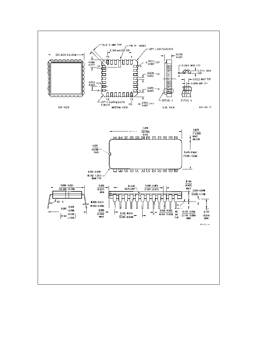
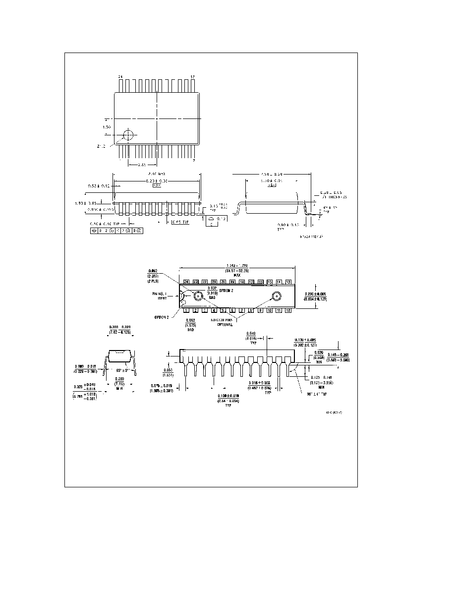
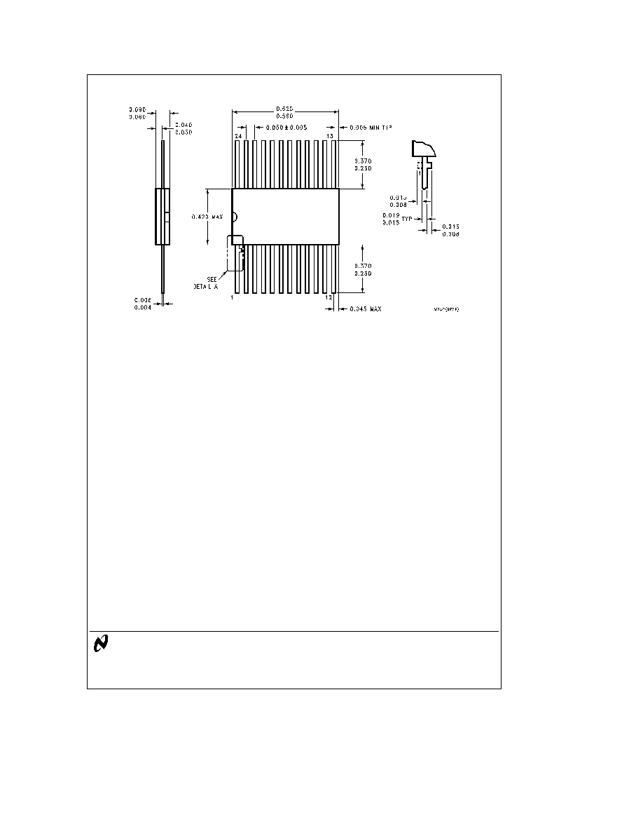
Physical Dimensions
inches (millimeters)
28-Lead Ceramic Leadless Chip Carrier (L)
NS Package Number E28A
24-Lead Ceramic Dual-In-Line Package (D)
NS Package Number J24A
7

Physical Dimensions
inches (millimeters) (Continued)
24-Lead (0 300 Wide) Ceramic Dual-In-Line Package (SD)
NS Package Number J24F
24-Lead (0 300 Wide) Molded Small Outline Package JEDEC (S)
NS Package Number M24B
8
Physical Dimensions
inches (millimeters) (Continued)
24-Lead Molded Shrink Small Outline EIAJ Type II (MSA)
NS Package Number MSA24
24-Lead (0 300 Wide) Molded Dual-In-Line Package (SP)
NS Package Number N24C
9
54F74F544
Octal
Registered
Transceiver
Physical Dimensions
inches (millimeters) (Continued)
24-Lead Ceramic Flatpak (F)
NS Package Number W24C
LIFE SUPPORT POLICY
NATIONAL'S PRODUCTS ARE NOT AUTHORIZED FOR USE AS CRITICAL COMPONENTS IN LIFE SUPPORT
DEVICES OR SYSTEMS WITHOUT THE EXPRESS WRITTEN APPROVAL OF THE PRESIDENT OF NATIONAL
SEMICONDUCTOR CORPORATION As used herein
1 Life support devices or systems are devices or
2 A critical component is any component of a life
systems which (a) are intended for surgical implant
support device or system whose failure to perform can
into the body or (b) support or sustain life and whose
be reasonably expected to cause the failure of the life
failure to perform when properly used in accordance
support device or system or to affect its safety or
with instructions for use provided in the labeling can
effectiveness
be reasonably expected to result in a significant injury
to the user
National Semiconductor
National Semiconductor
National Semiconductor
National Semiconductor
National Semiconductores
National Semiconductor
Corporation
GmbH
Japan Ltd
Hong Kong Ltd
Do Brazil Ltda
(Australia) Pty Ltd
2900 Semiconductor Drive
Livry-Gargan-Str 10
Sumitomo Chemical
13th Floor Straight Block
Rue Deputado Lacorda Franco
Building 16
P O Box 58090
D-82256 F4urstenfeldbruck
Engineering Center
Ocean Centre 5 Canton Rd
120-3A
Business Park Drive
Santa Clara CA 95052-8090
Germany
Bldg 7F
Tsimshatsui Kowloon
Sao Paulo-SP
Monash Business Park
Tel 1(800) 272-9959
Tel (81-41) 35-0
1-7-1 Nakase Mihama-Ku
Hong Kong
Brazil 05418-000
Nottinghill Melbourne
TWX (910) 339-9240
Telex 527649
Chiba-City
Tel (852) 2737-1600
Tel (55-11) 212-5066
Victoria 3168 Australia
Fax (81-41) 35-1
Ciba Prefecture 261
Fax (852) 2736-9960
Telex 391-1131931 NSBR BR
Tel (3) 558-9999
Tel (043) 299-2300
Fax (55-11) 212-1181
Fax (3) 558-9998
Fax (043) 299-2500
National does not assume any responsibility for use of any circuitry described no circuit patent licenses are implied and National reserves the right at any time without notice to change said circuitry and specifications