
TL F 9555
54F74F544
Octal
Registered
Transceiver
December 1994
54F 74F544
Octal Registered Transceiver
General Description
The 'F544 octal transceiver contains two sets of D-type
latches for temporary storage of data flowing in either direc-
tion Separate Latch Enable and Output Enable inputs are
provided for each register to permit independent control of
inputting and outputting in either direction of data flow The
A outputs are guaranteed to sink 24 mA (20 mA Mil) while
the B outputs are rated for 64 mA (48 mA Mil) The 'F544
inverts data in both directions
Features
Y
8-bit octal transceiver
Y
Back-to-back registers for storage
Y
Separate controls for data flow in each direction
Y
A outputs sink 24 mA (20 mA Mil) B outputs sink
64 mA (48 mA Mil)
Y
300 mil slim PDIP
Commercial
Military
Package
Package Description
Number
74F544SPC
N24C
24-Lead (0 300 Wide) Molded Dual-In-Line
54F544DM (Note 2)
J24A
24-Lead Ceramic Dual-In-Line
54F544SDM (Note 2)
J24F
24-Lead (0 300 Wide) Ceramic Dual-In-Line
74F544SC (Note 1)
M24B
24-Lead (0 300 Wide) Molded Small Outline JEDEC
74F544MSA (Note 1)
MSA24
24-Lead Molded Shrink Small Outline EIAJ Type II
54F544FM (Note 2)
W24C
24-Lead Cerpack
54F544LM (Note 2)
E28A
24-Lead Ceramic Leadless Chip Carrier Type C
Note 1
Devices also available in 13
reel Use suffix
e
SCX and MSAX
Note 2
Military grade device with environmental and burn-in processing Use suffix
e
DMQB FMQB and LMQB
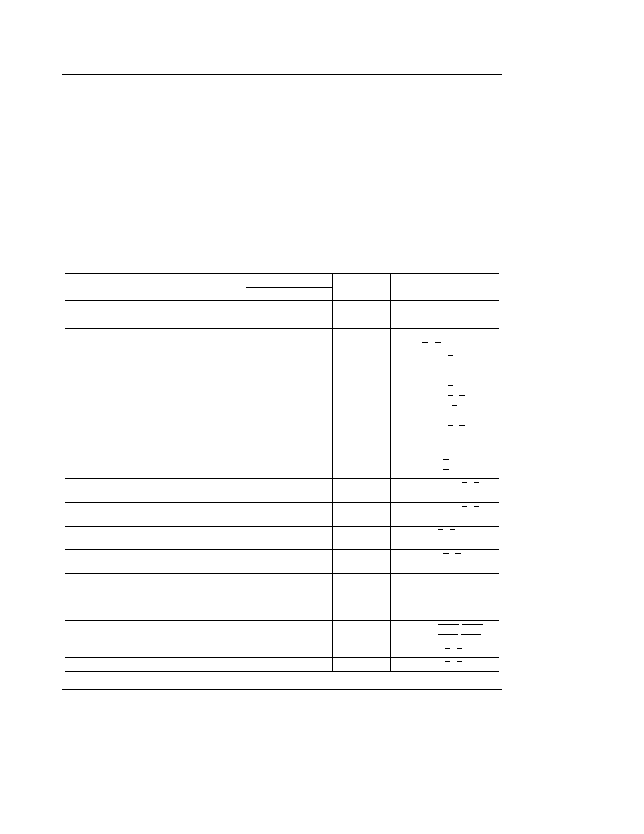
Logic Symbols
TL F 9555 � 2
IEEE IEC
TL F 9555 � 1
TRI-STATE
is a registered trademark of National Semiconductor Corporation
C1995 National Semiconductor Corporation
RRD-B30M75 Printed in U S A

Connection Diagrams
Pin Assignment for
DIP SOIC and Flatpak
TL F 9555 � 3
Pin Assignment
for LCC
TL F 9555 � 4
Unit Loading Fan Out
54F 74F
Pin Names
Description
U L
Input I
IH
I
IL
HIGH LOW
Output I
OH
I
OL
OEAB
A-to-B Output Enable Input (Active LOW)
1 0 1 0
20 mA
b
0 6 mA
OEBA
B-to-A Output Enable Input (Active LOW)
1 0 1 0
20 mA
b
0 6 mA
CEAB
A-to-B Enable Input (Active LOW)
1 0 2 0
20 mA
b
1 2 mA
CEBA
B-to-A Enable Input (Active LOW)
1 0 2 0
20 mA
b
1 2 mA
LEAB
A-to-B Latch Enable Input (Active LOW)
1 0 1 0
20 mA
b
0 6 mA
LEBA
B-to-A Latch Enable Input (Active LOW)
1 0 1 0
20 mA
b
0 6 mA
A
0
� A
7
A-to-B Data Inputs or
3 5 1 083
70 mA
b
650 mA
B-to-A TRI-STATE Outputs
150 40(33 3)
b
3 mA 24 mA (20 mA)
B
0
� B
7
B-to-A Data Inputs or
3 5 1 083
70 mA
b
650 mA
A-to-B TRI-STATE Outputs
600 106 6(80)
b
12 mA 64 mA (48 mA)
Functional Description
The 'F544 contains two sets of eight D-type latches with
separate input and output controls for each set For data
flow from A to B for example the A-to-B Enable (CEAB)
input must be LOW in order to enter data from A
0
� A
7
or
take data from B
0
� B
7
as indicated in the Data I O Control
Table With CEAB LOW a LOW signal on the A-to-B Latch
Enable (LEAB) input makes the A-to-B latches transparent
a subsequent LOW-to-HIGH transition of the LEAB signal
puts the A latches in the storage mode and their outputs no
longer change with the A inputs With CEAB and OEAB both
LOW the TRI-STATE
B output buffers are active and re-
flect the data present at the output of the A latches Control
of data flow from B to A is similar but using the CEBA
LEBA and OEBA inputs
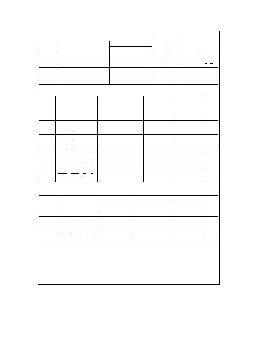
Data I O Control Table
Inputs
Latch Status
Output Buffers
CEAB
LEAB
OEAB
H
X
X
Latched
High Z
X
H
X
Latched
L
L
X
Transparent
X
X
H
High Z
L
X
L
Driving
H
e
HIGH Voltage Level
L
e
LOW Voltage Level
X
e
Immaterial
A-to-B data flow shown B-to-A flow control is the same
except using CEBA LEBA and OEBA
2

Logic Diagram
TL F 9555 � 5
Please note that this diagram is provided only for the understanding of logic operations and should not be used to estimate propagation delays
3
Absolute Maximum Ratings
(Note 1)
If Military Aerospace specified devices are required
please contact the National Semiconductor Sales
Office Distributors for availability and specifications
Storage Temperature
b
65 C to
a
150 C
Ambient Temperature under Bias
b
55 C to
a
125 C
Junction Temperature under Bias
b
55 C to
a
175 C
Plastic
b
55 C to
a
150 C
V
CC
Pin Potential to
Ground Pin
b
0 5V to
a
7 0V
Input Voltage (Note 2)
b
0 5V to
a
7 0V
Input Current (Note 2)
b
30 mA to
a
5 0 mA
Note 1
Absolute maximum ratings are values beyond which the device may
be damaged or have its useful life impaired Functional operation under
these conditions is not implied
Note 2
Either voltage limit or current limit is sufficient to protect inputs
Voltage Applied to Output
in HIGH State (with V
CC
e
0V)
Standard Output
b
0 5V to V
CC
TRI-STATE Output
b
0 5V to
a
5 5V
Current Applied to Output
in LOW State (Max)
twice the rated I
OL
(mA)
Recommended Operating
Conditions
Free Air Ambient Temperature
Military
b
55 C to
a
125 C
Commercial
0 C to
a
70 C
Supply Voltage
Military
a
4 5V to
a
5 5V
Commercial
a
4 5V to
a
5 5V
DC Electrical Characteristics
Symbol
Parameter
54F 74F
Units
V
CC
Conditions
Min
Typ
Max
V
IH
Input HIGH Voltage
2 0
V
Recognized as a HIGH Signal
V
IL
Input LOW Voltage
0 8
V
Recognized as a LOW Signal
V
CD
Input Clamp Diode Voltage
b
1 2
V
Min
I
IN
e b
18 mA
(except A
n
B
n
)
V
OH
Output HIGH
54F 10% V
CC
2 5
I
OH
e b
1 mA (A
n
)
Voltage
54F 10% V
CC
2 4
I
OH
e b
3 mA (A
n
B
n
)
54F 10% V
CC
2 0
I
OH
e b
12 mA (B
n
)
74F 10% V
CC
2 5
V
Min
I
OH
e b
1 mA (A
n
)
74F 10% V
CC
2 4
I
OH
e b
3 mA (A
n
B
n
)
74F 10% V
CC
2 0
I
OH
e b
15 mA (B
n
)
74F 5% V
CC
2 7
I
OH
e b
1 mA (A
n
)
74F 5% V
CC
2 7
I
OH
e b
3 mA (A
n
B
n
)
V
OL
Output LOW
54F 10% V
CC
0 5
I
OL
e
20 mA (A
n
)
Voltage
54F 10% V
CC
0 55
V
Min
I
OL
e
48 mA (B
n
)
74F 10% V
CC
0 5
I
OL
e
24 mA (A
n
)
74F 10% V
CC
0 55
I
OL
e
64 mA (B
n
)
I
IH
Input HIGH
54F
20 0
m
A
Max
V
IN
e
2 7V (except A
n
B
n
)
Current
74F
5 0
I
BVI
Input HIGH Current
54F
100
m
A
Max
V
IN
e
7 0V (except A
n
B
n
)
Breakdown Test
74F
7 0
I
BVIT
Input HIGH Current
54F
1 0
mA
Max
V
IN
e
5 5V (A
n
B
n
)
Breakdown (I O)
74F
0 5
I
CEX
Output HIGH
54F
250
m
A
Max
V
OUT
e
V
CC
(A
n
B
n
)
Leakage Current
74F
250
V
ID
Input Leakage
74F
4 75
V
0 0
I
ID
e
1 9 mA
Test
All Other Pins Grounded
I
OD
Output Leakage
74F
3 75
m
A
0 0
V
IOD
e
150 mV
Circuit Current
All Other Pins Grounded
I
IL
Input LOW Current
b
0 6
mA
Max
V
IN
e
0 5V (OEAB OEBA)
b
1 2
V
IN
e
0 5V (CEAB CEBA)
I
IH
a
I
OZH
Output Leakage Current
70
m
A
Max
V
OUT
e
2 7V (A
n
B
n
)
I
IL
a
I
OZL
Output Leakage Current
b
650
m
A
Max
V
OUT
e
0 5V (A
n
B
n
)
4
DC Electrical Characteristics
(Continued)
Symbol
Parameter
54F 74F
Units
V
CC
Conditions
Min
Typ
Max
I
OS
Output Short-Circuit Current
b
60
b
150
mA
Max
V
OUT
e
0V (A
n
)
b
100
b
225
V
OUT
e
0V (B
n
)
I
ZZ
Bus Drainage Test
500
m
A
0 0V
V
OUT
e
5 25V (A
n
B
n
)
I
CCH
Power Supply Current
70
105
mA
Max
V
O
e
HIGH
I
CCL
Power Supply Current
85
130
mA
Max
V
O
e
LOW
I
CCZ
Power Supply Current
83
125
mA
Max
V
O
e
HIGH Z
AC Electrical Characteristics
74F
54F
74F
T
A
e a
25 C
T
A
V
CC
e
Mil
T
A
V
CC
e
Com
Symbol
Parameter
V
CC
e a
5 0V
C
L
e
50 pF
C
L
e
50 pF
Units
C
L
e
50 pF
Min
Typ
Max
Min
Max
Min
Max
t
PLH
Propagation Delay
3 0
7 0
9 5
3 0
12 0
3 0
10 5
t
PHL
Transparent Mode
3 0
5 0
6 5
2 5
8 5
3 0
7 5
ns
A
n
to B
n
or B
n
to A
n
t
PLH
Propagation Delay
6 0
10 0
13 0
6 0
18 0
6 0
14 5
ns
t
PHL
LEBA to A
n
4 0
7 0
9 5
4 0
11 5
4 0
10 5
t
PLH
Propagation Delay
6 0
10 0
13 0
6 0
18 0
6 0
14 5
ns
t
PHL
LEAB to B
n
4 0
7 0
9 5
4 0
11 5
4 0
10 5
t
PZH
Output Enable Time
3 0
7 0
9 0
3 0
11 0
3 0
10 0
t
PZL
OEBA or OEAB to A
n
or B
n
4 0
7 5
10 5
4 0
13 0
4 0
12 0
CEBA or CEAB to A
n
or B
n
ns
t
PHZ
Output Disable Time
1 0
6 0
8 0
2 0
10 0
1 0
9 0
t
PLZ
OEBA or OEAB to A
n
or B
n
2 5
5 5
10 5
2 0
9 5
2 5
11 5
CEBA or CEAB to A
n
or B
n
AC Operating Requirements
74F
54F
74F
Symbol
Parameter
T
A
e a
25 C
T
A
V
CC
e
Mil
T
A
V
CC
e
Com
Units
V
CC
e a
5 0V
Min
Max
Min
Max
Min
Max
t
s
(H)
Setup Time HIGH or LOW
3 0
3 0
3 0
t
s
(L)
A
n
or B
n
to LEBA or LEAB
3 0
3 0
3 0
ns
t
h
(H)
Hold Time HIGH or LOW
3 0
3 0
3 0
t
h
(L)
A
n
or B
n
to LEBA or LEAB
3 0
3 0
3 0
t
w
(L)
Latch Enable B to A
6 0
9 0
7 5
ns
Pulse Width LOW
5