
TL F 9467
54F74F64
4-2-3-2-Input
AND-OR-Invert
Gate
November 1994
54F 74F64
4-2-3-2-Input AND-OR-Invert Gate
General Description
This device contains gates configured to perform a 4-2-3-2
input AND-OR-INVERT function
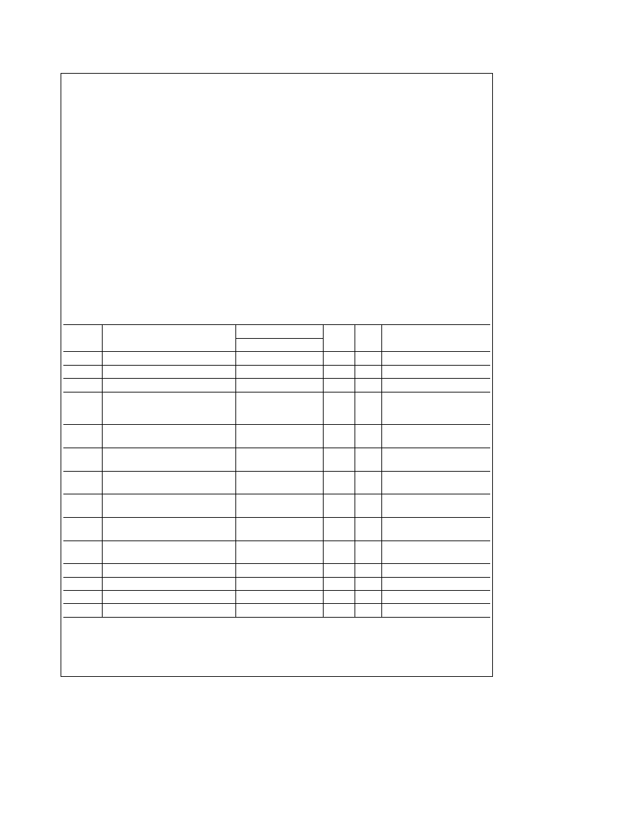
Commercial
Military
Package
Package Description
Number
74F64PC
N14A
14-Lead (0 300 Wide) Molded Dual-In-Line
54F64DM (Note 2)
J14A
14-Lead Ceramic Dual-In-Line
74F64SC (Note 1)
M14A
14-Lead (0 150 Wide) Molded Small Outline JEDEC
54F64FM (Note 2)
W14B
14-Lead Cerpack
54F64LM (Note 2)
E20A
20-Lead Ceramic Leadless Chip Carrier Type C
Note 1
Devices also available in 13
reel Use suffix
e
SCX
Note 2
Military grade device with environmental and burn-in processing Use suffix
e
DMQB FMQB and LMQB
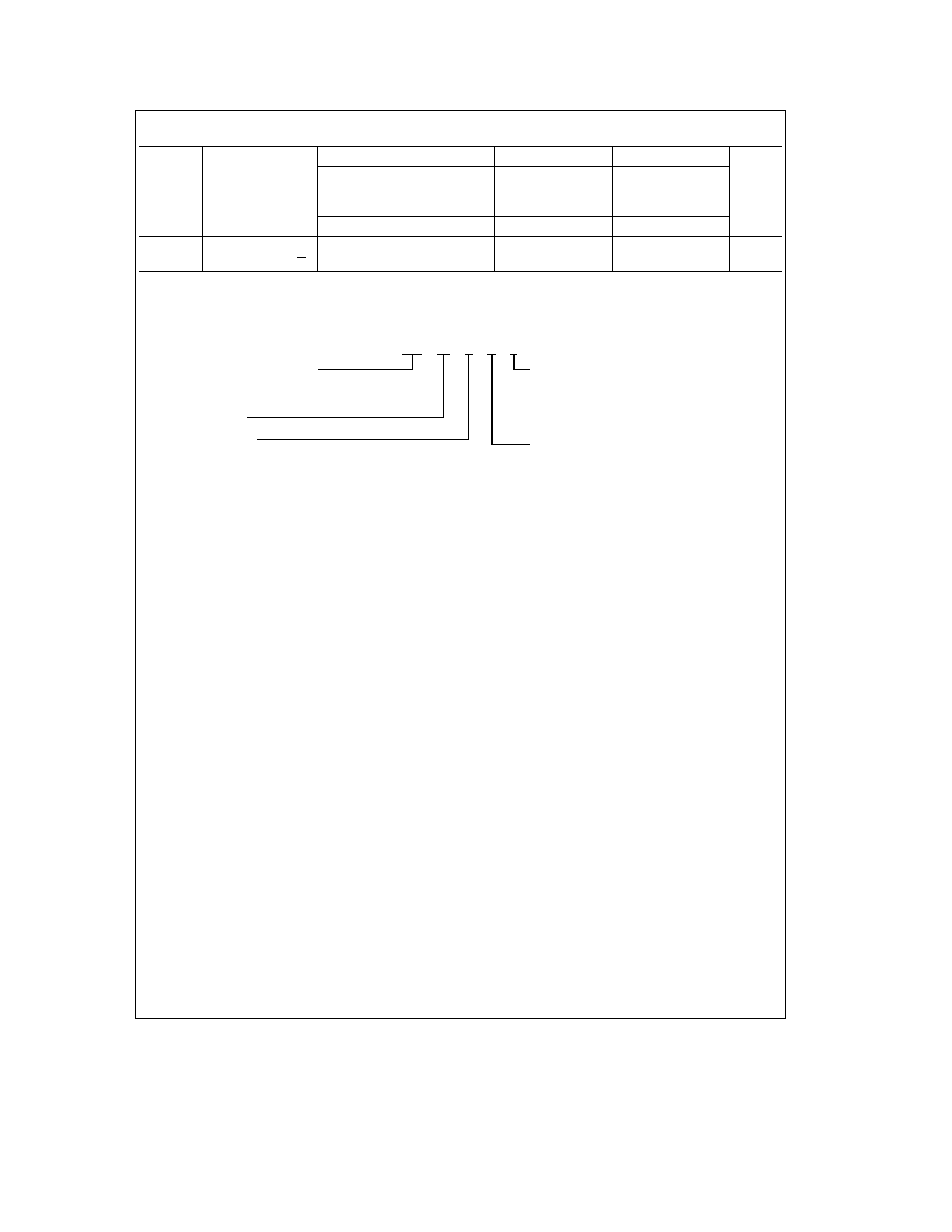
Logic Symbol
IEEE IEC
TL F 9467 � 3
Connection Diagrams
Pin Assignment for
DIP SOIC and Flatpak
TL F 9467 � 2
Pin Assignment
for LCC
TL F 9467 � 1
Unit Loading Fan Out
54F 74F
Pin Names
Description
U L
Input I
IH
I
IL
HIGH LOW
Output I
OH
I
OL
A
n
B
n
C
n
D
n
Inputs
1 0 1 0
20 mA
b
0 6 mA
O
Output
50 33 3
b
1 mA 20 mA
TRI-STATE
is a registered trademark of National Semiconductor Corporation
C1995 National Semiconductor Corporation
RRD-B30M105 Printed in U S A
Absolute Maximum Ratings
(Note 1)
If Military Aerospace specified devices are required
please contact the National Semiconductor Sales
Office Distributors for availability and specifications
Storage Temperature
b
65 C to
a
150 C
Ambient Temperature under Bias
b
55 C to
a
125 C
Junction Temperature under Bias
b
55 C to
a
175 C
Plastic
b
55 C to
a
150 C
V
CC
Pin Potential to
Ground Pin
b
0 5V to
a
7 0V
Input Voltage (Note 2)
b
0 5V to
a
7 0V
Input Current (Note 2)
b
30 mA to
a
5 0 mA
Voltage Applied to Output
in HIGH State (with V
CC
e
0V)
Standard Output
b
0 5V to V
CC
TRI-STATE Output
b
0 5V to
a
5 5V
Current Applied to Output
in LOW State (Max)
twice the rated I
OL
(mA)
Note 1
Absolute maximum ratings are values beyond which the device may
be damaged or have its useful life impaired Functional operation under
these conditions is not implied
Note 2
Either voltage limit or current limit is sufficient to protect inputs
Recommended Operating
Conditions
Free Air Ambient Temperature
Military
b
55 C to
a
125 C
Commercial
0 C to
a
70 C
Supply Voltage
Military
a
4 5V to
a
5 5V
Commercial
a
4 5V to
a
5 5V
DC Electrical Characteristics
Symbol
Parameter
54F 74F
Units
V
CC
Conditions
Min
Typ
Max
V
IH
Input HIGH Voltage
2 0
V
Recognized as a HIGH Signal
V
IL
Input LOW Voltage
0 8
V
Recognized as a LOW Signal
V
CD
Input Clamp Diode Voltage
b
1 2
V
Min
I
IN
e b
18 mA
V
OH
Output HIGH
54F 10% V
CC
2 5
I
OH
e b
1 mA
Voltage
74F 10% V
CC
2 5
V
Min
I
OH
e b
1 mA
74F 5% V
CC
2 7
I
OH
e b
1 mA
V
OL
Output LOW
54F 10% V
CC
0 5
V
Min
I
OL
e
20 mA
Voltage
74F 10% V
CC
0 5
I
OL
e
20 mA
I
IH
Input HIGH
54F
20 0
m
A
Max
V
IN
e
2 7V
Current
74F
5 0
I
BVI
Input HIGH Current
54F
100
m
A
Max
V
IN
e
7 0V
Breakdown Test
74F
7 0
I
CEX
Output High
54F
250
m
A
Max
V
OUT
e
V
CC
Leakage Current
74F
50
V
ID
Input Leakage
74F
4 75
V
0 0
I
ID
e
1 9 mA
Test
All Other Pins Grounded
I
OD
Output Leakage
74F
3 75
m
A
0 0
V
IOD
e
150 mV
Circuit Current
All Other Pins Grounded
I
IL
Input LOW Current
b
0 6
mA
Max
V
IN
e
0 5V
I
OS
Output Short-Circuit Current
b
60
b
150
mA
Max
V
OUT
e
0V
I
CCH
Power Supply Current
1 9
2 8
mA
Max
V
O
e
HIGH
I
CCL
Power Supply Current
3 1
4 7
mA
Max
V
O
e
LOW
2
AC Electrical Characteristics
74F
54F
74F
T
A
e a
25 C
T
A
V
CC
e
Mil
T
A
V
CC
e
Com
Symbol
Parameter
V
CC
e a
5 0V
C
L
e
50 pF
C
L
e
50 pF
Units
C
L
e
50 pF
Min
Typ
Max
Min
Max
Min
Max
t
PLH
Propagation Delay
2 5
4 6
6 5
2 5
8 5
2 5
7 5
ns
t
PHL
A
n
B
n
C
n
D
n
to O
1 5
3 2
4 5
1 5
6 5
1 5
5 5
Ordering Information
The device number is used to form part of a simplified purchasing code where the package type and temperature range are
defined as follows
74F
64
S
C
X
Temperature Range Family
Special Variations
74F
e
Commercial
QB
e
Military grade device with
54F
e
Military
environmental and burn-in
processing
Device Type
X
e
Devices shipped in 13 reel
Package Code
Temperature Range
P
e
Plastic DIP
C
e
Commercial (0 C to
a
70 C)
D
e
Ceramic DIP
M
e
Military (
b
55 C to
a
125 C)
F
e
Flatpak
L
e
Leadless Chip Carrier (LCC)
S
e
Small Outline SOIC
3
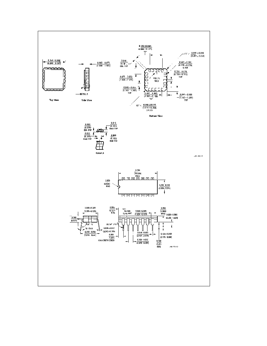
Physical Dimensions
inches (millimeters)
20-Lead Ceramic Leadless Chip Carrier (L)
NS Package Number E20A
14-Lead Ceramic Dual-In-Line Package (D)
NS Package Number J14A
4
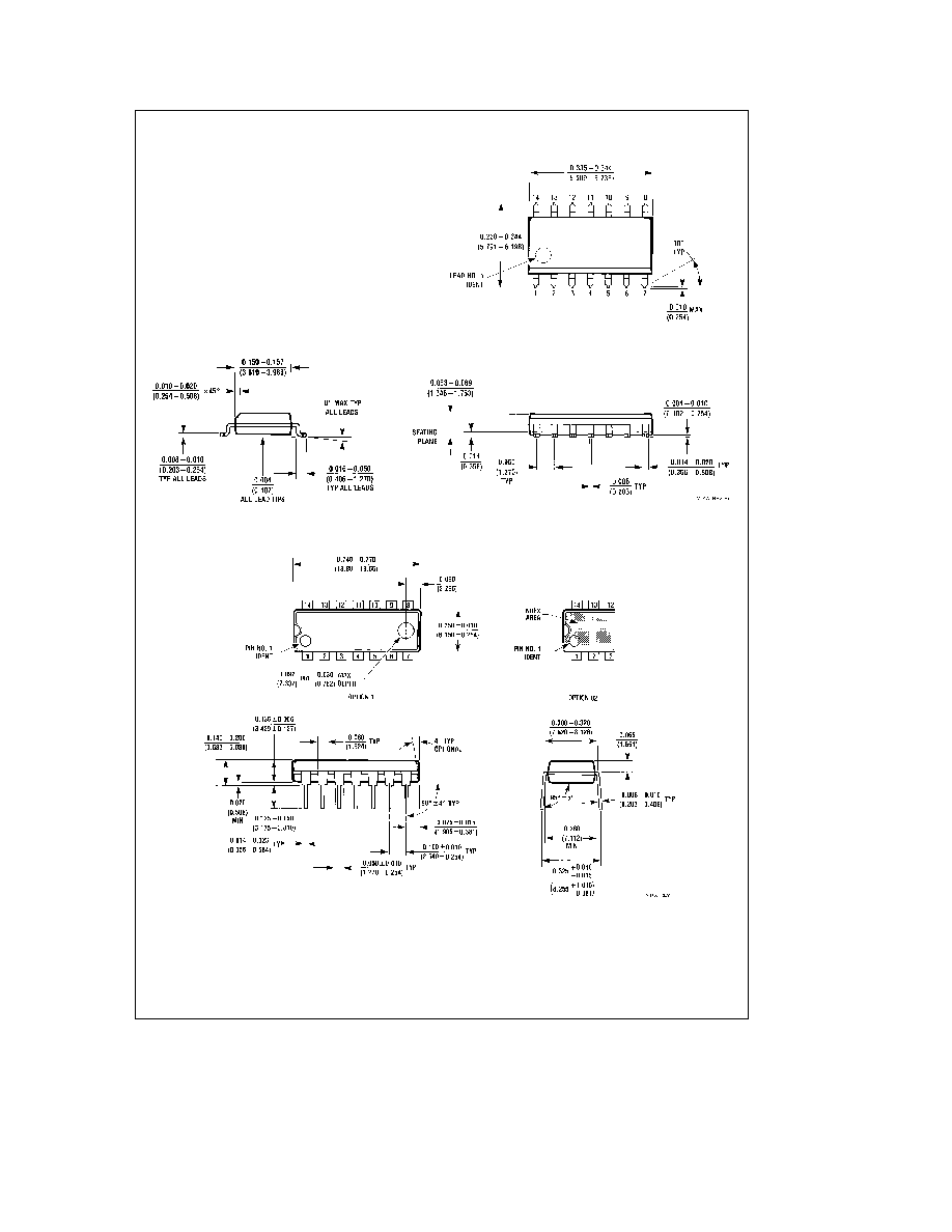
Physical Dimensions
inches (millimeters) (Continued)
14-Lead (0 150 Wide) Molded Small Outline JEDEC (S)
NS Package Number M14A
14-Lead (0 300 Wide) Molded Dual-In-Line Package (P)
NS Package Number N14A
5