
54FCT574
Octal D-Type Flip-Flop with TRI-STATE
Æ
Outputs
General Description
The 'FCT574 is an octal flip-flop with a buffered common
Clock (CP) and a buffered common Output Enable (OE). The
information presented to the D inputs is stored in the
flip-flops on the LOW-to-HIGH Clock (CP) transition.
The device is functionally identical to the 'FCT374 except for
the pinouts.
Features
n
Inputs and outputs on opposite sides of package
allowing easy interface with microprocessors
n
Useful as input or output port for microprocessors
n
Functionally identical to 'FCT374
n
TRI-STATE outputs for bus-oriented applications
n
Output sink capability of 32 mA, source capability of
12 mA
n
TTL input and output level compatible
n
CMOS power consumption
n
Standard Microcircuit Drawing (SMD) 5962-8951301
Ordering Code
Military
Package Number
Package Description
54FCT574DMQB
J20A
20-Lead Ceramic Dual-In-Line
54FCT574FMQB
W20A
20-Lead Cerpack
54FCT574LMQB
E20A
20-Lead Ceramic Leadless Chip Carrier, Type C
Connection Diagrams
Pin Descriptions
Pin
Description
Names
D
0
≠D
7
Data Inputs
CP
Clock Pulse Input
(Active Rising Edge)
OE
TRI-STATE Output Enable
Input (Active LOW)
O
0
≠O
7
TRI-STATE Outputs
TRI-STATE
Æ
is a registered trademark of National Semiconductor Corporation.
Pin Assignment for DIP and Flatpak
DS100966-1
Pin Assignment
for LCC
DS100966-2
October 1999
54FCT574
Octal
D-T
ype
Flip-Flop
with
TRI-ST
A
T
E
Outputs
© 1999 National Semiconductor Corporation
DS100966
www.national.com

Functional Description
The 'FCT574 consists of eight edge-triggered flip-flops with
individual D-type inputs and TRI-STATE true outputs. The
buffered clock and buffered Output Enable are common to all
flip-flops. The eight flip-flops will store the state of their indi-
vidual D inputs that meet the setup and hold times require-
ments on the LOW-to-HIGH Clock (CP) transition. With the
Output Enable (OE) LOW, the contents of the eight flip-flops
are available at the outputs. When OE is HIGH, the outputs
are in a high impedance state. Operation of the OE input
does not affect the state of the flip-flops.
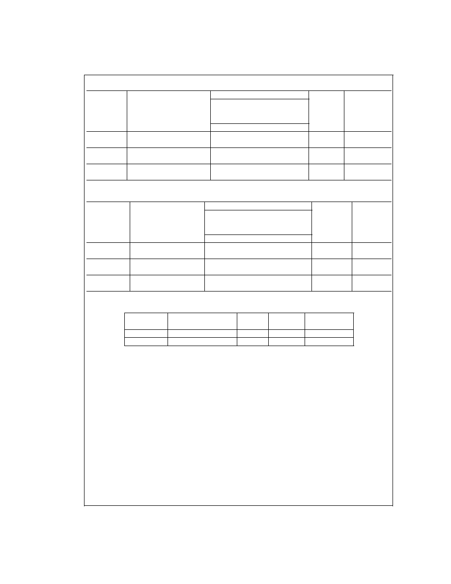
Function Table
Inputs
Internal Outputs
Function
OE
CP
D
Q
O
H
H or L
L
NC
Z
Hold
Inputs
Internal Outputs
Function
OE
CP
D
Q
O
H
H or L
H
NC
Z
Hold
H
N
L
L
Z
Load
H
N
H
H
Z
Load
L
N
L
L
L
Data Available
L
N
H
H
H
Data Available
L
H or L
L
NC
NC
No Change in Data
L
H or L
H
NC
NC
No Change in Data
H = HIGH Voltage Level
L = LOW Voltage Level
X = Immaterial
Z = High Impedance
N = LOW-to-HIGH Transition
NC = No Change
Logic Diagram
DS100966-3
Please note that this diagram is provided only for the understanding of logic operations and should not be used to estimate propagation delays.
54FCT574
www.national.com
2

Absolute Maximum Ratings
(Note 1)
If Military/Aerospace specified devices are required,
please contact the National Semiconductor Sales Office/
Distributors for availability and specifications.
Storage Temperature
-65∞C to +150∞C
Ambient Temperature under Bias
-55∞C to +125∞C
Junction Temperature under Bias
Ceramic
-55∞C to +175∞C
V
CC
Pin Potential to Ground Pin
-0.5V to +7.0V
Input Voltage (Note 2)
-0.5V to +7.0V
Input Current (Note 2)
-30 mA to +5.0 mA
Voltage Applied to Any Output in
the Disabled or Power-Off State
-0.5V to 5.5V
in the HIGH State
-0.5V to V
CC
Current Applied to Output
in LOW State (Max)
twice the rated I
OL
(mA)
DC Latchup Source Current
-500 mA
Recommended Operating
Conditions
Free Air Ambient Temperature
Military
-55∞C to +125∞C
Supply Voltage
Military
+4.5V to +5.5V
Note 1: Absolute maximum ratings are values beyond which the device may
be damaged or have its useful life impaired. Functional operation under these
conditions is not implied.
Note 2: Either voltage limit or current limit is sufficient to protect inputs.
DC Electrical Characteristics
Symbol
Parameter
FCT574
Units
V
CC
Conditions
Min
Max
V
IH
Input HIGH Voltage
2.0
V
Recognized HIGH Signal
V
IL
Input LOW Voltage
0.8
V
Recognized LOW Signal
V
CD
Input Clamp Diode Voltage
-1.2
V
Min
I
IN
= -18 mA
V
OH
Output HIGH
Voltage
54FCT
4.3
V
Min
I
OH
= -300 µA
54FCT
2.4
V
Min
I
OH
= -12 mA
V
OL
Output LOW Voltage
54FCT
0.2
V
Min
I
OL
= 300 µA
54FCT
0.5
V
Min
I
OL
= 32mA
I
IH
Input HIGH Current
5
µA
Max
V
IN
= 2.7V (Note 3)
5
V
IN
= V
CC
I
IL
Input LOW Current
-5
µA
Max
V
IN
= 0.5V (Note 3)
-5
V
IN
= 0.0V
I
OZH
Output Leakage Current
10
µA
0 - 5.5V
V
OUT
= 2.7V; OE = 2.0V
I
OZL
Output Leakage Current
-10
µA
0 - 5.5V
V
OUT
= 0.5V; OE = 2.0V
I
OS
Output Short-Circuit Current
-60
mA
Max
V
OUT
= 0.0V
I
CCQ
Power Supply Current
1.5
mA
Max
V
IN
= 0.2V or V
IN
= 5.3V, f
I
=
0MHz
I
CC
Power Supply Current
2.0
mA
Max
V
IN
= 3.4V
I
CCT
Additional
I
CC
/Input
6.0
mA
Max
V
I
= V
CC
- 2.1V or V
IN
= GND, f
CP
= 10MHz, Outputs open, OE =
GND, one bit toggling at f
I
= 5MHz,
50% duty cycle
5.5
mA
Max
V
I
= 5.3V or V
CC
= 0.2V, f
CP
=
10MHz, Outputs open, OE = GND,
one bit toggling at f
I
= 5MHz, 50%
duty cycle
I
CCD
Dynamic I
CC
No Load
0.40
mA/
MHz
Max
Outputs Open, OE = GND, One bit
toggling, 50% duty cycle, V
IN
=
5.3V or V
IN
= 0.2V
Note 3: Guaranteed, but not tested.
54FCT574
www.national.com
3
AC Electrical Characteristics
54FCT
Fig.
No.
T
A
= -55∞C to +125∞C
Symbol
Parameter
V
CC
= 4.5V to 5.5V
Units
C
L
= 50 pF
Min
Max
t
PLH
Propagation Delay
2.0
11.0
ns
Figure 4
t
PHL
CP to O
n
2.0
11.0
t
PZH
Output Enable Time
1.5
14.0
ns
Figure 6
t
PZL
1.5
14.0
t
PHZ
Output Disable Time
1.5
8.0
ns
Figure 6
t
PLZ
1.5
8.0
AC Operating Requirements
54FCT
T
A
= -55∞C to +125∞C
Fig.
Symbol
Parameter
V
CC
= 4.5V to 5.5V
Units
No.
C
L
= 50 pF
Min
Max
t
s
(H)
Setup Time, HIGH
3.5
ns
Figure 7
t
s
(L)
or LOW D
n
to CP
3.5
t
h
(H)
Hold Time, HIGH
2.0
ns
Figure 7
t
h
(L)
or LOW D
n
to CP
2.0
t
w
(H)
Pulse Width, CP,
7.0
ns
Figure 5
t
w
(L)
HIGH or LOW
7.0
Capacitance
Symbol
Parameter
Typ
Units
Conditions
T
A
= 25∞C
C
IN
Input Capacitance
5.0
pF
V
CC
= 0V
C
OUT
(Note 4)
Output Capacitance
9.0
pF
V
CC
= 5.0V
Note 4: C
OUT
is measured at frequency f = 1 MHz, per MIL-STD-883B, Method 3012.
54FCT574
www.national.com
4

AC Loading
DS100966-4
*Includes jig and probe capacitance
FIGURE 1. Standard AC Test Load
DS100966-6
FIGURE 2. V
M
= 1.5V
Input Pulse Requirements
Amplitude
Rep. Rate
t
w
t
r
t
f
3.0V
1 MHz
500 ns
2.5 ns
2.5 ns
FIGURE 3. Test Input Signal Requirements
DS100966-8
FIGURE 4. Propagation Delay Waveforms for
Inverting and Non-Inverting Functions
DS100966-5
FIGURE 5. Propagation Delay,
Pulse Width Waveforms
DS100966-7
FIGURE 6. TRI-STATE Output HIGH
and LOW Enable and Disable Times
DS100966-9
FIGURE 7. Setup Time, Hold Time
and Recovery Time Waveforms
54FCT574
www.national.com
5