TL F 8753
DP8216DP8216MDP8226DP8226M
4-Bit
Bidirectional
Bus
Transceivers
June 1990
DP8216 DP8216M DP8226 DP8226M
4-Bit Bidirectional Bus Transceivers
General Description
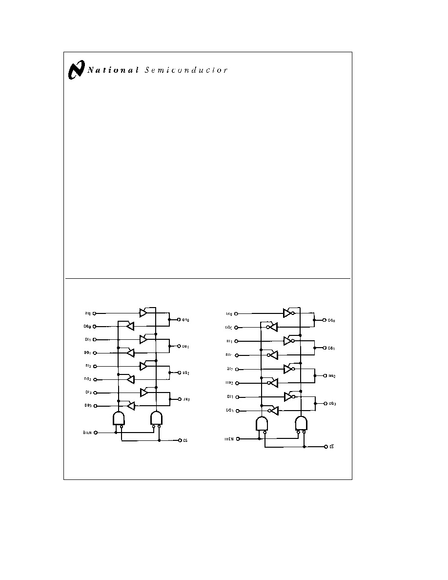
The DP8216 DP8216M and DP8226 DP8226M are 4-bit bi-
directional bus drivers to use in bus oriented applications
The
non-inverting
DP8216 DP8216M
and
inverting
DP8226 DP8226M drivers are provided for flexibility in sys-
tem design
Each buffered line of the four-bit drivers consists of two
separate buffers that are TRI-STATE
to achieve direct bus
interface and bidirectional capability On one side of the
driver the output of one buffer and the input of another are
tied together (DB) this side is used to interface to the sys-
tem side components such as memories I O etc because
its interface is TTL compatible and it has high driver (50
mA) On the other side of the driver the inputs and outputs
are separated to provide maximum flexibility Of course
they can be tied together so that the driver can be used to
buffer a true bidirectional bus The DO outputs on this side
of the driver have a special high voltage output drive capa-
bility so that direct interface to the 8080 type CPUs is
achieved with an adequate amount of noise immunity
The CS input is a device enable When it is ``high'' the out-
put drivers are all forced to their high-impedance state
When it is a ``low'' the device is enabled and the direction of
the data flow is determined by the DIEN input
The DIEN input controls the direction of data flow which is
accomplished by forcing one of the pair of buffers into its
high-impedance state and allowing the other to transmit its
data A simple two-gate circuit is used for this function
Features
Y
Data bus buffer driver to 8080 type CPUs
Y
Low input load current
0 25 mA maximum
Y
High output drive capability for driving system data
bus
50 mA at 0 5V
Y
Power up-down protection
Y
DP8216 DP8216M have non-inverting outputs
Y
DP8226 DP8226M have inverting outputs
Y
Output high voltage compatible with direct interface to
MOS
Y
TRI-STATE outputs
Y
Advanced Schottky processing
Y
Available in military and commercial temperature
Logic Diagrams
DP8216 DP8216M
TL F 8753 � 1
DP8226 DP8226M
TL F 8753 � 2
TRI-STATE
is a registered trademark of National Semiconductor Corp
C1995 National Semiconductor Corporation
RRD-B30M105 Printed in U S A

Absolute Maximum Ratings
(Note 1)
If Military Aerospace specified devices are required
please contact the National Semiconductor Sales
Office Distributors for availability and specifications
Min
Max
Units
All Output and Supply Voltages
b
0 5
a
7 0
V
All Input Voltages
b
1 0
a
5 5
V
Output Currents
125
mA
Maximum Power Dissipation at 25 C
Cavity Package
1509
mW
Molded Package
1476
mW
Note
Derate cavity package 10 1 mW C above 25 C derate molded
package 11 8 mW C above 25 C
Min
Max Units
Storage Temperature
b
65
a
150
C
Lead Temperature (soldering 4 seconds)
260
C
Operating Conditions
Min
Max
Units
Supply Voltage V
CC
DP8216M DP8226M
4 5
5 5
V
DP8216 DP8226
4 75
5 25
V
Temperature T
A
DP8216M DP8226M
b
55
a
125
C
DP8216 DP8226
0
a
70
C
Electrical Characteristics
DP8216 DP8226 V
CC
e
5V
g
5% (Notes 2 3 and 4)
Symbol
Parameter
Conditions
Limits
Units
Min
Typ
Max
DRIVERS
V
IL
Input Low Voltage
0 95
V
V
IH
Input High Voltage
2
V
I
F
Input Load Current
V
F
e
0 45V
b
0 03
b
0 25
mA
I
R
Input Leakage Current
V
R
e
5 25V
10
m
A
V
C
Input Clamp Voltage
I
C
e b
5 mA
b
1 2
V
V
OL1
Output Low Voltage
I
OL
e
25 mA
0 3
0 45
V
V
OL2
Output Low Voltage
DP8216 I
OL
e
55 mA
0 5
0 6
V
DP8226 I
OL
e
50 mA
V
OH
Output High Voltage
I
OH
e b
10 mA
2 4
3 0
V
I
SC
Output Short Circuit Current
V
CC
e
5V
b
30
b
75
b
120
mA
l
I
O
l
Output Leakage Current TRI-STATE
V
O
e
0 45V 5 5V
100
m
A
RECEIVERS
V
IL
Input Low Voltage
0 95
V
V
IH
Input High Voltage
2
V
I
F
Input Load Current
V
F
e
0 45V
b
0 08
b
0 25
mA
V
C
Input Clamp Voltage
I
C
e b
5 mA
b
1 2
V
V
OL
Output Low Voltage
I
OL
e
15 mA
0 3
0 45
V
V
OH1
Output High Voltage
I
OH
e b
1 mA
3 65
4 0
V
I
SC
Output Short Circuit Current
V
CC
e
5V
b
15
b
35
b
65
mA
l
I
O
l
Output Leakage Current TRI-STATE
V
O
e
0 45V 5 5V
20
m
A
CONTROL INPUTS (CS DIEN)
V
IL
Input Low Voltage
0 95
V
V
IH
Input High Voltage
2
V
I
F
Input Load Current
V
F
e
0 45V
b
0 15
b
0 5
mA
I
R
Input Leakage Current
V
R
e
5 25V
20
m
A
I
CC
Power Supply Current
DP8216
95
130
mA
DP8226
85
120
mA
2

Electrical Characteristics
(Continued) DP8216M DP8226M V
CC
e
5V
g
10% (Notes 2 3 and 4)
Symbol
Parameter
Conditions
Limits
Units
Min
Typ
Max
DRIVERS
V
IL
Input Low Voltage
DP8216M
0 95
V
DP8226M
0 90
V
V
IH
Input High Voltage
2
V
I
F
Input Load Current
V
F
e
0 45V
b
0 08
b
0 25
mA
I
R
Input Leakage Current
V
R
e
5 5V
40
m
A
V
C
Input Clamp Voltage
I
C
e b
5 mA
b
1 2
V
V
OL1
Output Low Voltage
I
OL
e
25 mA
0 3
0 45
V
V
OL2
Output Low Voltage
I
OL
e
45 mA
0 5
0 6
V
V
OH
Output High Voltage
I
OH
e b
5 mA
2 4
3 0
V
I
SC
Output Short Circuit Current
V
CC
e
5 0V
b
30
b
75
b
120
mA
l
I
O
l
Output Leakage Current TRI-STATE
V
O
e
0 45V 5 5V
100
m
A
RECEIVERS
V
IL
Input Low Voltage
DP8216M
0 95
V
DP8226M
0 9
V
V
IH
Input High Voltage
2
V
I
F
Input Load Current
V
F
e
0 45V
b
0 08
b
0 25
mA
V
C
Input Clamp Voltage
I
C
e b
5 mA
b
1 2
V
V
OL
Output Low Voltage
I
OL
e
15 mA
0 3
0 45
V
V
OH1
Output High Voltage
I
OH
e b
0 5 mA
3 4
3 8
V
V
OH2
Output High Voltage
I
OH
e b
2 mA
2 4
V
I
SC
Output Short Circuit Current
V
CC
e
5 0V
b
15
b
35
b
65
mA
l
I
O
l
Output Leakage Current TRI-STATE
V
O
e
0 45V 5 5V
20
m
A
CONTROL INPUTS (CS DIEN)
V
IL
Input Low Voltage
DP8216M
0 95
V
DP8226M
0 9
V
V
IH
Input High Voltage
2
V
I
F
Input Load Current
V
F
e
0 45V
b
0 15
b
0 5
mA
I
R
Input Leakage Current
V
R
e
5 5V
80
m
A
I
CC
Power Supply Current
DP8216M
95
130
mA
DP8226M
85
120
mA
3
Switching Characteristics
(Notes 2 3 and 4)
Symbol
Parameter
Conditions
Limits
Units
Min
Typ
Max
DP8216M DP8226M V
CC
e
5V
g
10%
t
PD1
Input to Output Delay DO Outputs
C
L
e
30 pF R
1
e
300X
15
25
ns
R
2
e
600X
t
PD2
Input to Output Delay DB Outputs
C
L
e
300 pF R
1
e
90X
DP8216M
R
2
e
180X
19
33
ns
DP8226M
16
25
ns
t
E
Output Enable Time
DO Outputs C
L
e
30 pF
DP8216M
R
1
e
300X
42
75
ns
DP8226M
R
2
e
600X
36
62
ns
DB Outputs C
L
e
300 pF
R
1
e
90X
R
2
e
180X
t
D
Output Disable Time
DO Outputs C
L
e
5 pF
DP8216M
R
1
e
300X
16
40
ns
DP8226M
R
2
e
600X
16
38
ns
DB Outputs C
L
e
5 pF
R
1
e
90X
R
2
e
180X
DP8216 DP8226 V
CC
e
5 0V
g
5%
t
PD1
Input to Output Delay DO Outputs
C
L
e
30 pF R
1
e
300X
15
25
ns
R
2
e
600X
t
PD2
Input to Output Delay DB Outputs
C
L
e
300 pF R
1
e
90X
DP8216
R
2
e
180X
20
30
ns
DP8226
16
25
ns
t
E
Output Enable Time
DO Outputs C
L
e
30 pF
DP8216
R
1
e
300X
45
65
ns
DP8226
R
2
e
600X
35
54
ns
DB Outputs C
L
e
300 pF
R
1
e
90X
R
2
e
180X
t
D
Output Disable Time
DO Outputs C
L
e
5 pF
R
1
e
300X
R
2
e
600X
20
35
ns
DB Outputs C
L
e
5 pF
R
1
e
90X
R
2
e
180X
Note 1
``Absolute Maximum Ratings'' are those values beyond which the safety of the device cannot be guaranteed They are not meant to imply that the
devices should be operated at these limits The tables of ``Electrical Characteristics'' provide conditions for actual device operation
Note 2
Unless otherwise specified min max limits apply across the
b
55 C to
a
125 C temperature range for the DP8216M and DP8226M and across the
0 C to
a
70 C temperature range for the DP8216 and DP8226 All typical values are given for V
CC
e
5V and T
A
e
25 C
Note 3
All currents into device pins are positive all currents out of device pins are negative All voltages are referenced to ground unless otherwise specified
Note 4
Only one output at a time should be shorted
4
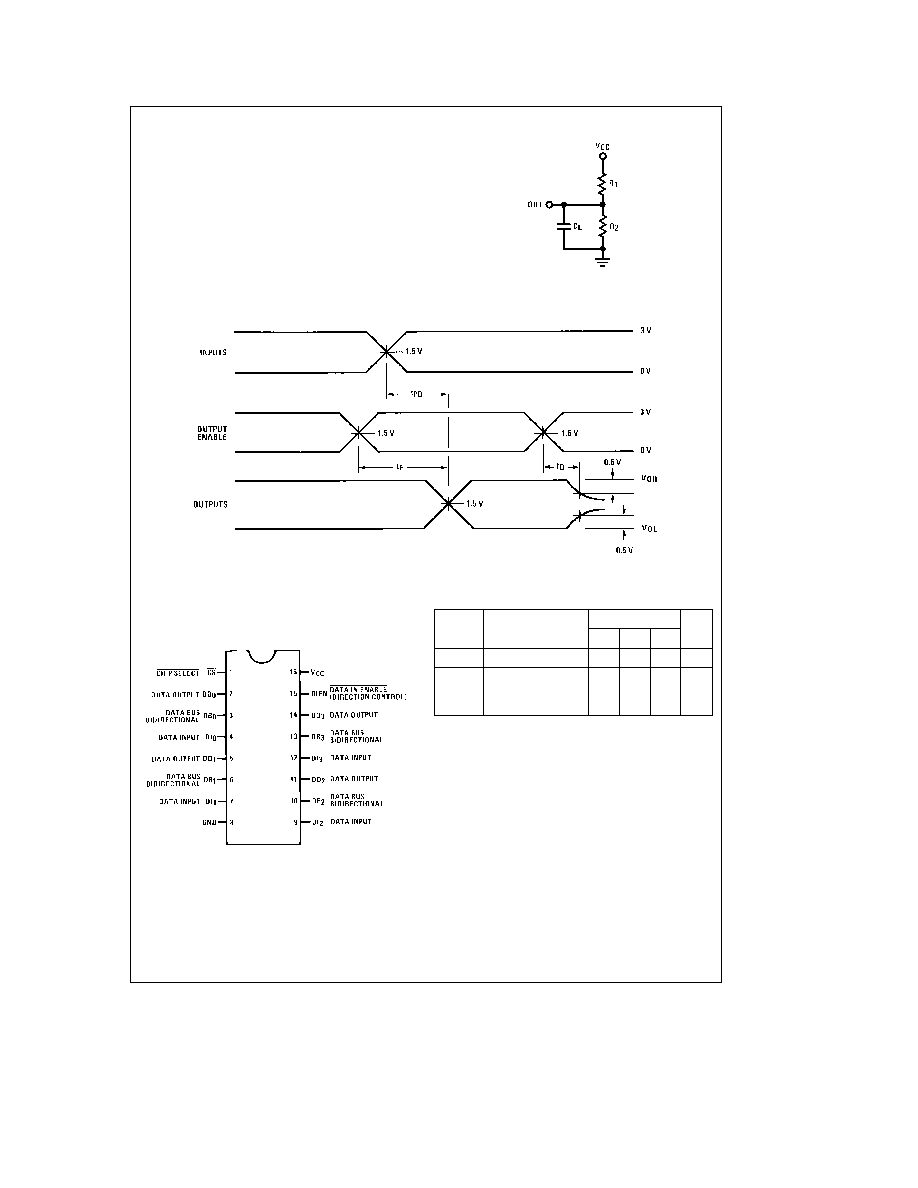
Test Conditions
Input rise and fall times of 5 0 ns between 1 0V and 2 0V
Output loading is 5 0 mA and 10 pF
Speed measurements are made at 1 5V levels
Test Load Circuit
TL F 8753 � 4
Switching Time Waveforms
TL F 8753 � 5
Connection Diagram
Dual-In-Line Package
TL F 8753 � 3
Order Number DP8216J DP8216N DP8226J DP8226N
DP8216MJ or DP8226MJ
See NS Package Number J16A or N16A
Capacitance
T
A
e
25 C
Symbol
Parameter
Limit
Unit
Min
Typ
Min
C
IN
Input Capacitance
4
6
pF
C
OUT
Output Capacitance
DO Outputs
6
10
pF
DO Outputs
13
18
pF
Note
This parameter is periodically sampled and is not 100% tested Condi-
tion of measurement is f
e
1 MHz V
BIAS
e
2 5V V
CC
e
5 0V and T
A
e
25 C
5
DP8216DP8216MDP8226DP8226M
4-Bit
Bidirectional
Bus
Transceivers
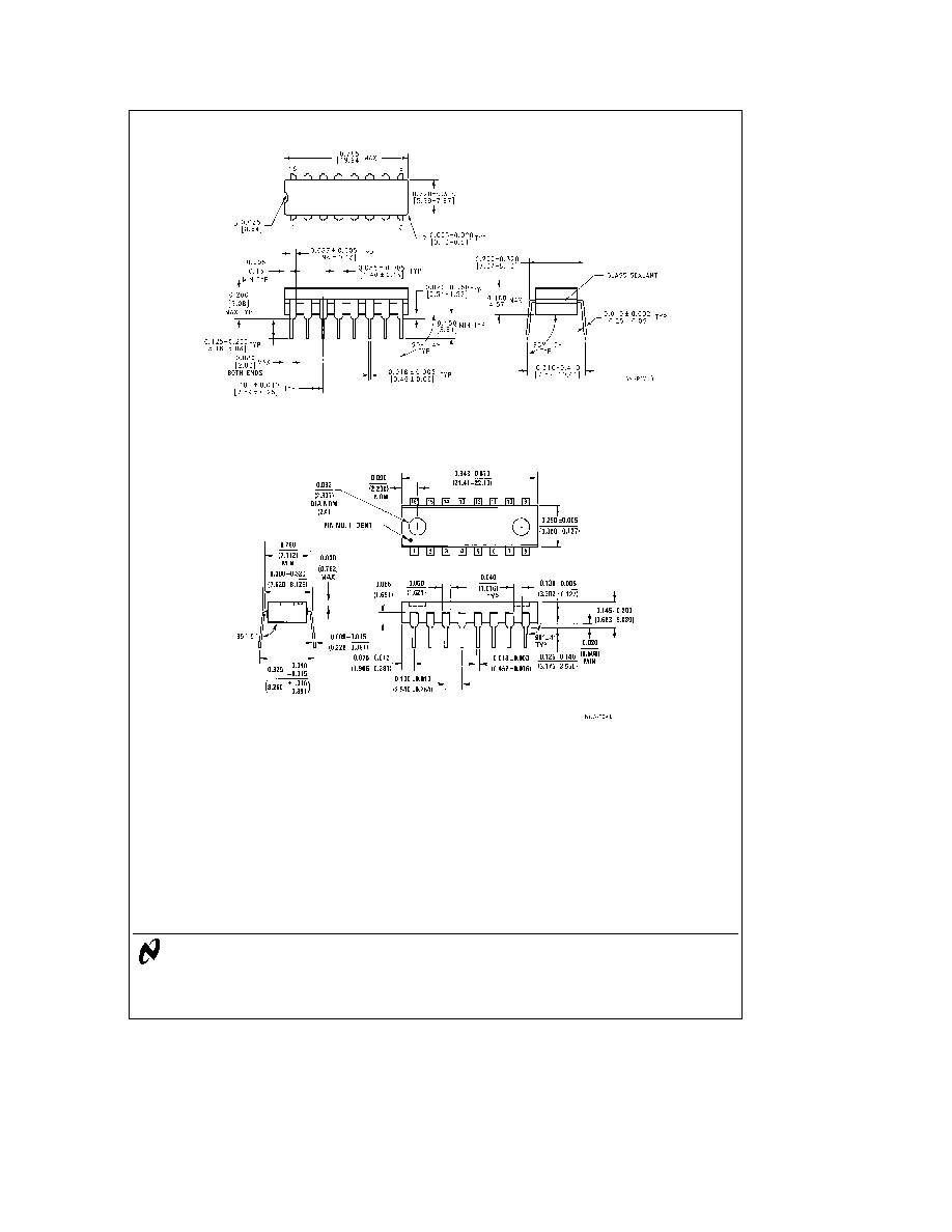
Physical Dimensions
inches (millimeters)
Ceramic Dual-In-Line Package (J)
Order Number DP8216J DP8226J DP8216MJ or DP8226MJ
NS Package Number J16A
Molded Dual-In-Line Package (N)
Order Number DP8216N or DP8226N
NS Package N16A
LIFE SUPPORT POLICY
NATIONAL'S PRODUCTS ARE NOT AUTHORIZED FOR USE AS CRITICAL COMPONENTS IN LIFE SUPPORT
DEVICES OR SYSTEMS WITHOUT THE EXPRESS WRITTEN APPROVAL OF THE PRESIDENT OF NATIONAL
SEMICONDUCTOR CORPORATION As used herein
1 Life support devices or systems are devices or
2 A critical component is any component of a life
systems which (a) are intended for surgical implant
support device or system whose failure to perform can
into the body or (b) support or sustain life and whose
be reasonably expected to cause the failure of the life
failure to perform when properly used in accordance
support device or system or to affect its safety or
with instructions for use provided in the labeling can
effectiveness
be reasonably expected to result in a significant injury
to the user
National Semiconductor
National Semiconductor
National Semiconductor
National Semiconductor
Corporation
Europe
Hong Kong Ltd
Japan Ltd
1111 West Bardin Road
Fax (a49) 0-180-530 85 86
13th Floor Straight Block
Tel 81-043-299-2309
Arlington TX 76017
Email cnjwge tevm2 nsc com
Ocean Centre 5 Canton Rd
Fax 81-043-299-2408
Tel 1(800) 272-9959
Deutsch Tel (a49) 0-180-530 85 85
Tsimshatsui Kowloon
Fax 1(800) 737-7018
English
Tel (a49) 0-180-532 78 32
Hong Kong
Fran ais Tel (a49) 0-180-532 93 58
Tel (852) 2737-1600
Italiano
Tel (a49) 0-180-534 16 80
Fax (852) 2736-9960
National does not assume any responsibility for use of any circuitry described no circuit patent licenses are implied and National reserves the right at any time without notice to change said circuitry and specifications