TL F 6398
54LS164DM54LS164DM74LS164
8-Bit
Serial
InParallel
Out
Shift
Registers
June 1989
54LS164 DM54LS164 DM74LS164
8-Bit Serial In Parallel Out Shift Registers
General Description
These 8-bit shift registers feature gated serial inputs and an
asynchronous clear A low logic level at either input inhibits
entry of the new data and resets the first flip-flop to the low
level at the next clock pulse thus providing complete con-
trol over incoming data A high logic level on either input
enables the other input which will then determine the state
of the first flip-flop Data at the serial inputs may be changed
while the clock is high or low but only information meeting
the setup and hold time requirements will be entered Clock-
ing occurs on the low-to-high level transition of the clock
input All inputs are diode-clamped to minimize transmis-
sion-line effects
Features
Y
Gated (enable disable) serial inputs
Y
Fully buffered clock and serial inputs
Y
Asynchronous clear
Y
Typical clock frequency 36 MHz
Y
Typical power dissipation 80 mW
Y
Alternate Military Aerospace device (54LS164) is avail-
able Contact a National Semiconductor Sales Office
Distributor for specifications
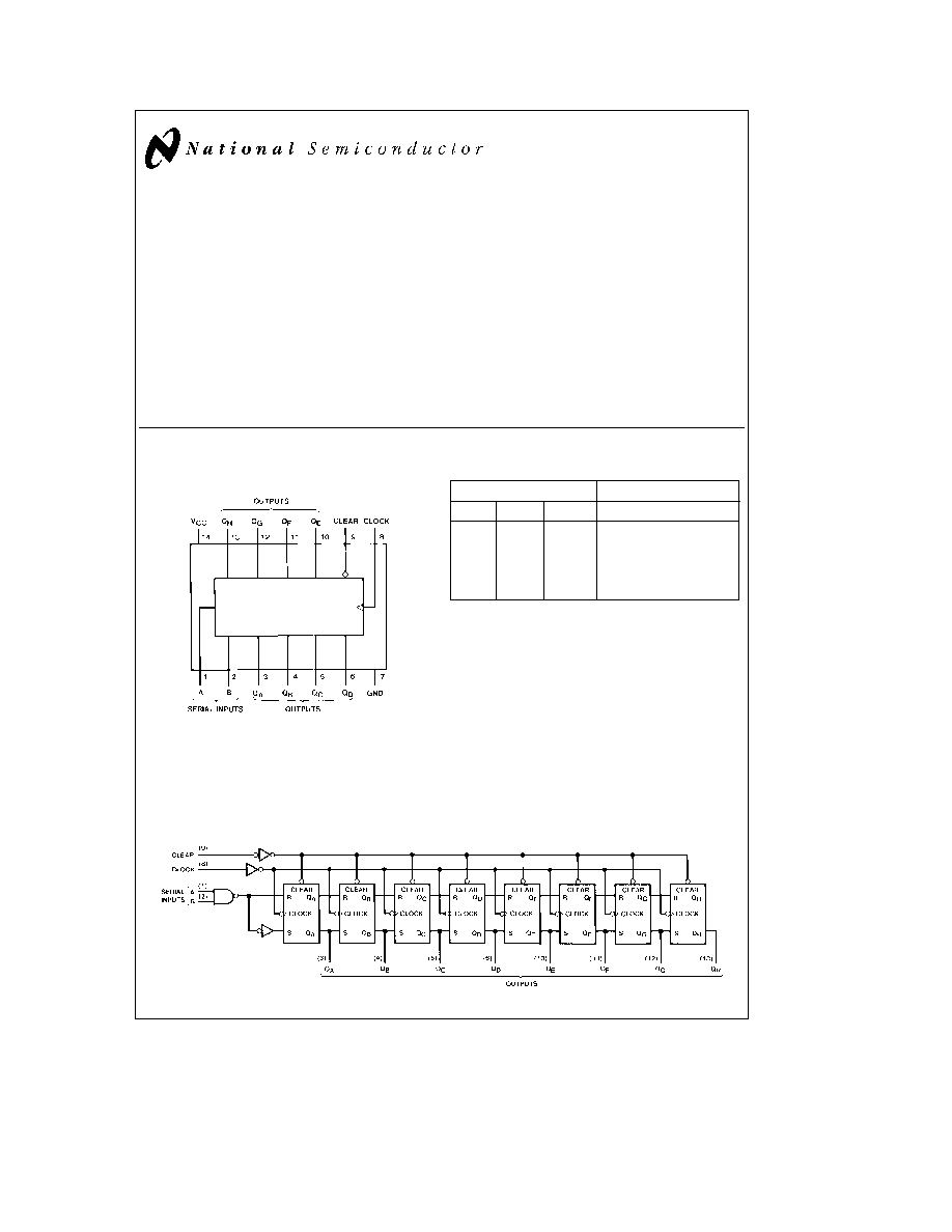
Connection Diagram
Dual-In-Line Package
TL F 6398 ≠ 1
Order Number 54LS164DMQB 54LS164FMQB
54LS164LMQB DM54LS164J DM54LS164W
DM74LS164M or DM74LS164N
See NS Package Number E20A
J14A M14A N14A or W14B
Function Table
Inputs
Outputs
Clear
Clock
A
B
Q
A
Q
B
Q
H
L
X
X
X
L
L
L
H
L
X
X
Q
A0
Q
B0
Q
H0
H
u
H
H
H
Q
An
Q
Gn
H
u
L
X
L
Q
An
Q
Gn
H
u
X
L
L
Q
An
Q
Gn
H
e
High Level (steady state) L
e
Low Level (steady state)
X
e
Don't Care (any input including transitions)
u
e
Transition from low to high level
Q
A0
Q
B0
Q
H0
e
The level of Q
A
Q
B
or Q
H
respectively before the
indicated steady-state input conditions were established
Q
An
Q
Gn
e
The level of Q
A
or Q
G
before the most recent
u
transition of
the clock indicates a one-bit shift
Logic Diagram
TL F 6398 ≠ 2
C1995 National Semiconductor Corporation
RRD-B30M105 Printed in U S A

Absolute Maximum Ratings
(Note)
If Military Aerospace specified devices are required
please contact the National Semiconductor Sales
Office Distributors for availability and specifications
Supply Voltage
7V
Input Voltage
7V
Operating Free Air Temperature Range
DM54LS and 54LS
b
55 C to
a
125 C
DM74LS
0 C to
a
70 C
Storage Temperature Range
b
65 C to
a
150 C
Note
The ``Absolute Maximum Ratings'' are those values
beyond which the safety of the device cannot be guaran-
teed The device should not be operated at these limits The
parametric values defined in the ``Electrical Characteristics''
table are not guaranteed at the absolute maximum ratings
The ``Recommended Operating Conditions'' tables will de-
fine the conditions for actual device operation
Recommended Operating Conditions
Symbol
Parameter
DM54LS164
DM74LS164
Units
Min
Nom
Max
Min
Nom
Max
V
CC
Supply Voltage
4 5
5
5 5
4 75
5
5 25
V
V
IH
High Level Input Voltage
2
2
V
V
IL
Low Level Input Voltage
0 7
0 8
V
I
OH
High Level Output Current
b
0 4
b
0 4
mA
I
OL
Low Level Output Current
4
8
mA
f
CLK
Clock Frequency (Note 4)
0
25
0
25
MHz
t
W
Pulse Width
Clock
20
20
ns
(Note 4)
Clear
20
20
t
SU
Data Setup Time (Note 4)
17
17
ns
t
H
Data Hold Time (Note 4)
5
5
ns
t
REL
Clear Release Time (Note 4)
30
30
ns
T
A
Free Air Operating Temperature
b
55
125
0
70
C
Electrical Characteristics
over recommended operating free air temperature range (unless otherwise noted)
Symbol
Parameter
Conditions
Min
Typ
Max
Units
(Note 1)
V
I
Input Clamp Voltage
V
CC
e
Min I
I
e b
18 mA
b
1 5
V
V
OH
High Level Output
V
CC
e
Min I
OH
e
Max
DM54
2 5
3 4
V
Voltage
V
IL
e
Max V
IH
e
Min
DM74
2 7
3 4
V
OL
Low Level Output
V
CC
e
Min I
OL
e
Max
DM54
0 25
0 4
Voltage
V
IL
e
Max V
IH
e
Min
DM74
0 35
0 5
V
I
OL
e
4 mA V
CC
e
Min
DM74
0 25
0 4
I
I
Input Current
Max
V
CC
e
Max V
I
e
7V
0 1
mA
Input Voltage
I
IH
High Level Input Current
V
CC
e
Max V
I
e
2 7V
20
m
A
I
IL
Low Level Input Current
V
CC
e
Max V
I
e
0 4V
b
0 4
mA
I
OS
Short Circuit
V
CC
e
Max
DM54
b
20
b
100
mA
Output Current
(Note 2)
DM74
b
20
b
100
I
CC
Supply Current
V
CC
e
Max (Note 3)
16
27
mA
Note 1
All typicals are at V
CC
e
5V T
A
e
25 C
Note 2
Not more than one output should be shorted at a time and the duration should not exceed one second
Note 3
I
CC
is measured with all outputs open the SERIAL input grounded the CLOCK input at 2 4V and a momentary ground then 4 5V applied to the CLEAR
input
Note 4
T
A
e
25 C and V
CC
e
5V
2
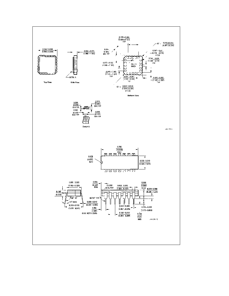
Physical Dimensions
inches (millimeters)
Ceramic Leadless Chip Carrier Package (E)
Order Number 54LS164LMQB
NS Package Number E20A
14-Lead Ceramic Dual-In-Line Package (J)
Order Number 54LS164DMQB or DM54LS164J
NS Package Number J14A
4

Physical Dimensions
inches (millimeters) (Continued)
14-Lead Small Outline Molded Package (M)
Order Number DM74LS164M
NS Package Number M14A
14-Lead Molded Dual-In-Line Package (N)
Order Number DM74LS164N
NS Package Number N14A
5
