TL F 10186
54LS379DM74LS379
Quad
Parallel
Register
with
Enable
June 1989
54LS379 DM74LS379
Quad Parallel Register with Enable
General Description
The LS379 is a 4-bit register with buffered common Enable
This device is similar to the LS175 but features the common
Enable rather than common Master Reset
Features
Y
Edge-triggered D-type inputs
Y
Buffered positive edge-triggered clock
Y
Buffered common enable input
Y
True and complement outputs
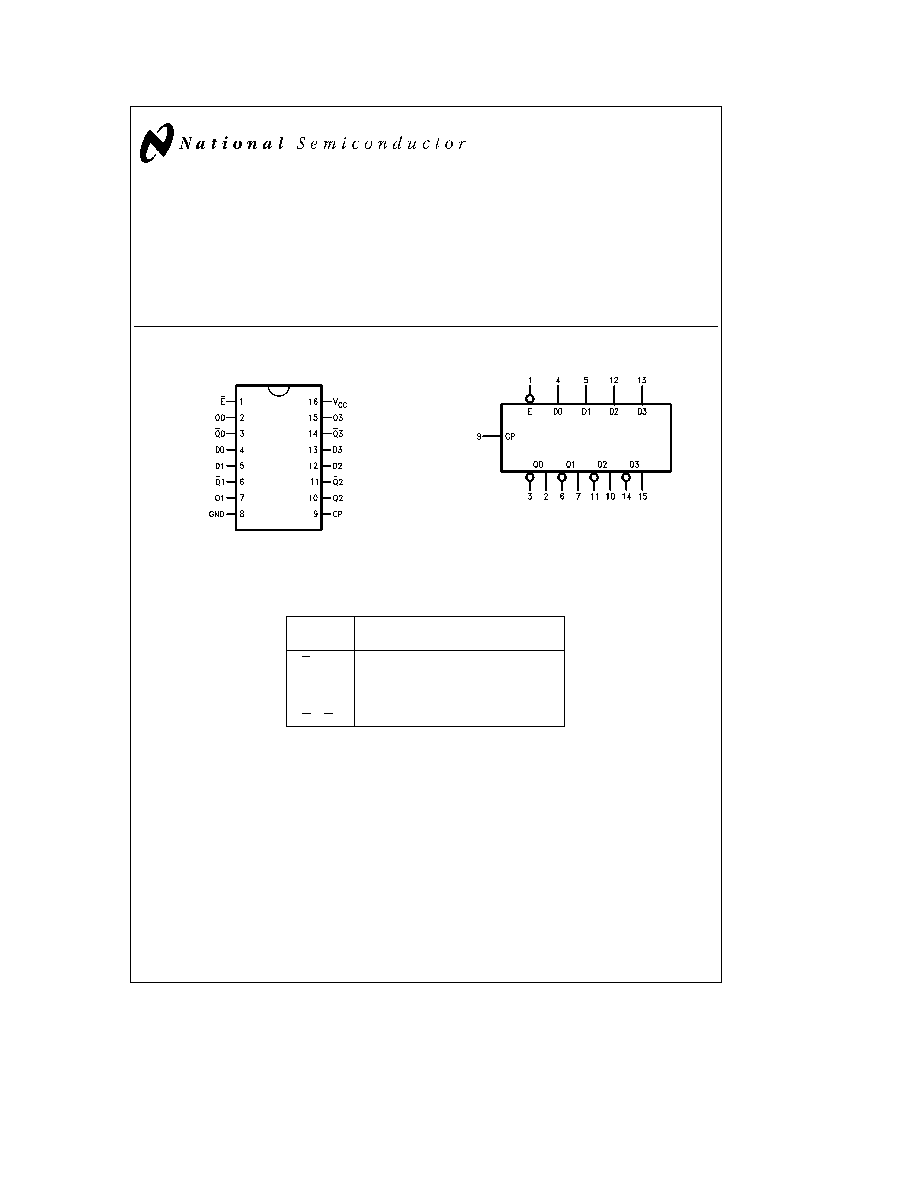
Connection Diagram
Dual-In-Line Package
TL F 10186 ≠ 1
Order Number 54LS379DMQB 54LS379FMQB
54LS379LMQB DM74LS379M or DM74LS379N
See NS Package Number E20A
J16A M16A N16E or W16A
Logic Symbol
TL F 10186 ≠ 2
V
CC
e
Pin 16
GND
e
Pin 8
Pin
Description
Names
E
Enable Input (Active LOW)
D0 ≠ D3
Data Inputs
CP
Clock Pulse Input (Active Rising Edge)
Q0 ≠ Q3
Flip-Flop Outputs
Q0 ≠ Q3
Complement Outputs
C1995 National Semiconductor Corporation
RRD-B30M105 Printed in U S A

Absolute Maximum Ratings
(Note)
If Military Aerospace specified devices are required
please contact the National Semiconductor Sales
Office Distributors for availability and specifications
Supply Voltage
7V
Input Voltage
7V
Operating Free Air Temperature Range
54LS
b
55 C to
a
125 C
DM74LS
0 C to
a
70 C
Storage Temperature Range
b
65 C to
a
150 C
Note
The ``Absolute Maximum Ratings'' are those values
beyond which the safety of the device cannot be guaran-
teed The device should not be operated at these limits The
parametric values defined in the ``Electrical Characteristics''
table are not guaranteed at the absolute maximum ratings
The ``Recommended Operating Conditions'' table will define
the conditions for actual device operation
Recommended Operating Conditions
Symbol
Parameter
54LS379
DM74LS379
Units
Min
Nom
Max
Min
Nom
Max
V
CC
Supply Voltage
4 5
5
5 5
4 75
5
5 25
V
V
IH
High Level Input Voltage
2
2
V
V
IL
Low Level Input Voltage
0 7
0 8
V
I
OH
High Level Output Current
b
0 4
b
0 4
mA
I
OL
Low Level Output Current
4
8
mA
T
A
Free Air Operating Temperature
b
55
125
0
70
C
t
s
(H)
Setup Time HIGH or LOW
20
20
ns
t
s
(L)
Dn to CP
t
h
(H)
Hold Time HIGH or LOW
5
5
ns
t
h
(L)
Dn to CP
t
s
(H)
Setup Time HIGH or LOW
25
25
ns
t
s
(L)
E to CP
t
h
(H)
Hold Time HIGH or LOW
5
5
ns
t
h
(L)
E to CP
t
w
(L)
CP Pulse Width LOW
17
17
ns
Electrical Characteristics
over recommended operating free air temperature range (unless otherwise noted)
Symbol
Parameter
Conditions
Min
Typ
Max
Units
(Note 1)
V
I
Input Clamp Voltage
V
CC
e
Min I
I
e b
18 mA
b
1 5
V
V
OH
High Level Output
V
CC
e
Min I
OH
e
Max
54LS
2 5
V
Voltage
V
IL
e
Max
DM74
2 7
V
OL
Low Level Output
V
CC
Min I
OL
e
Max
54LS
0 4
Voltage
V
IH
e
Min
DM74
0 5
V
I
OL
e
4 mA V
CC
e
Min
DM74
0 4
I
I
Input Current
Max
V
CC
e
Max V
I
e
10V
0 1
mA
Input Voltage
I
IH
High Level Input Current
V
CC
e
Max V
I
e
2 7V
20
m
A
I
IL
Low Level Input Current
V
CC
e
Max V
I
e
0 4V
b
0 4
mA
I
OS
Short Circuit
V
CC
e
Max
54LS
b
20
b
100
mA
Output Current
(Note 2)
DM74
b
20
b
100
I
CC
Supply Current
V
CC
e
Max
18
mA
Note 1
All typicals are at V
CC
e
5V T
A
e
25 C
Note 2
Note more than one output should be shorted at a time and the duration should not exceed one second
2
Switching Characteristics
V
CC
e a
5 0V T
A
e a
25 C (See Section 1 for test waveforms and output load)
Symbol
Parameter
R
L
e
2 kX C
L
e
15 pF
Units
Min
Max
f
max
Maximum Clock Frequency
30
MHz
t
PLH
Propagation Delay
27
ns
t
PHL
CP to Qn
27
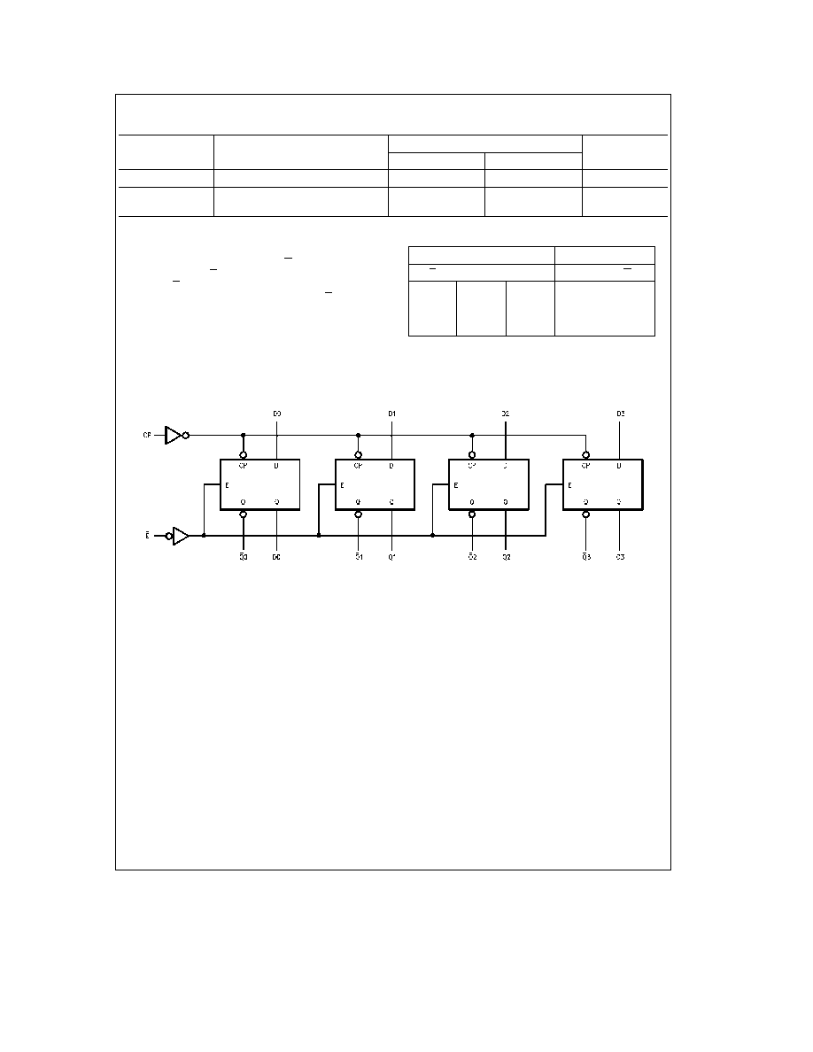
Functional Description
The LS379 consists of four edge-triggered D-type flip-flops
with individual D inputs and Q and Q outputs The Clock
(CP) and Enable (E) inputs are common to all flip-flops
When the E input is HIGH the register will retain the present
data independent of the CP input The Dn and E inputs can
change when the clock is in either state provided that the
recommended setup and hold times are observed
Truth Table
Inputs
Outputs
E
CP
Dn
Qn
Qn
H
L
X
No
No
Change
Change
L
L
H
H
L
L
L
L
L
H
H
e
HIGH Voltage Level
L
e
LOW Voltage Level
X
e
Immaterial
Logic Diagram
TL F 10186 ≠ 3
3
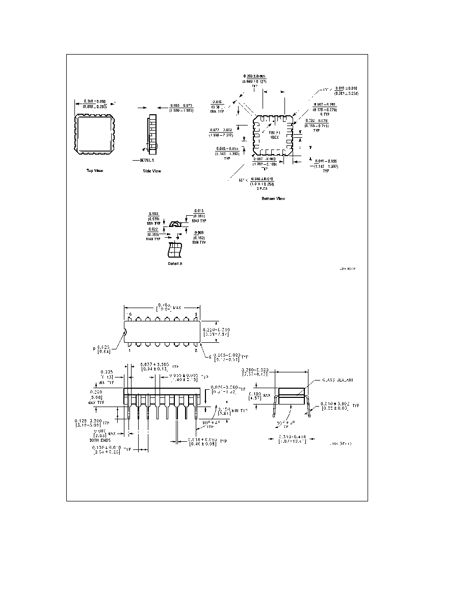
Physical Dimensions
inches (millimeters)
Ceramic Leadless Chip Carrier Package (E)
Order Number 54LS379LMQB
NS Package Number E20A
16-Lead Ceramic Dual-In-Line Package (J)
Order Number 54LS379DMQB
NS Package Number J16A
4
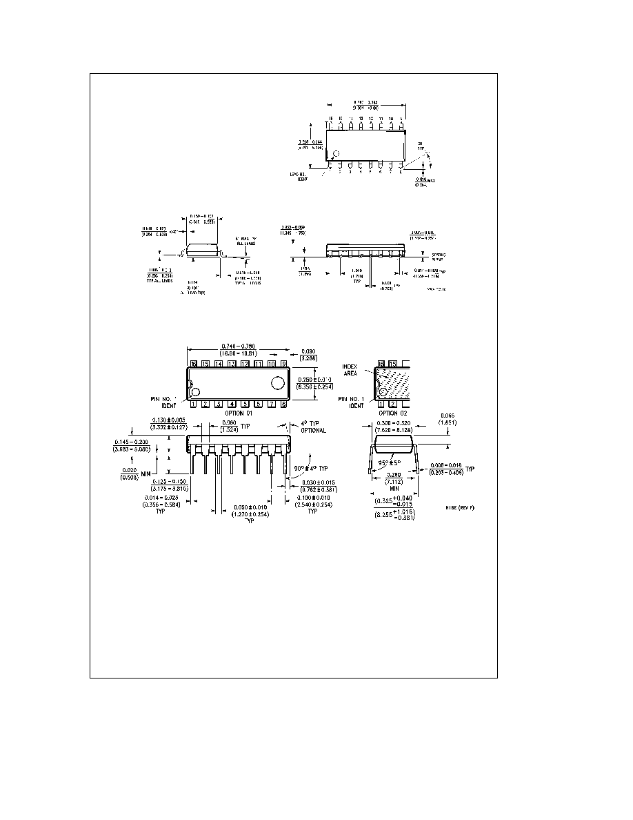
Physical Dimensions
inches (millimeters)
16-Lead Small Outline Molded Package (M)
Order Number DM74LS379M
NS Package Number M16A
16-Lead Molded Dual-In-Line Package (N)
Order Number DM74LS379N
NS Package Number N16E
5