
54LVX3383
10-Bit Low Power Bus-Exchange Switch
General Description
The 54LVX3383 provides two sets of high-speed CMOS
TTL-compatible bus switches. The low on resistance of the
switch allows inputs to be connected to outputs without add-
ing propagation delay or generating additional ground
bounce noise. The device operates as a 10-bit bus switch or
a 5-bit bus exchanger. The bus exchange (BX) signal pro-
vides nibble swapping of the AB and CD pairs of signals.
This exchange configuration allows byte swapping of buses
in systems. It can also be used as a quad 2-to-1 multiplexer
and to create low delay barrel shifters. The bus enable (BE )
signal turns the switches on.
Features
n
5
switch connection between two ports
n
Minimal propagation delay through the switch
n
Ultra low power with 0.2 µA typical I
CC
n
Zero ground bounce in flow-through mode
n
Control inputs compatible with TTL level
n
Available in CDIP and Flatpack packages
n
Standard Microcircuit Drawing (SMD) 5962-9950601
Ordering Code
Order Number
Package Number
Package Description
54LVX3383J-QML
J24F
24-Lead Ceramic Dual-in-line
54LVX3383W-QML
W24C
24-Lead Cerpack
Logic Diagram
Connection Diagram
DS011652-1
Pin Assignment for
CDIP and Cerpack
DS011652-2
May 1999
54L
VX3383
10-Bit
Low
Power
Bus-Exchange
Switch
© 1999 National Semiconductor Corporation
DS011652
www.national.com
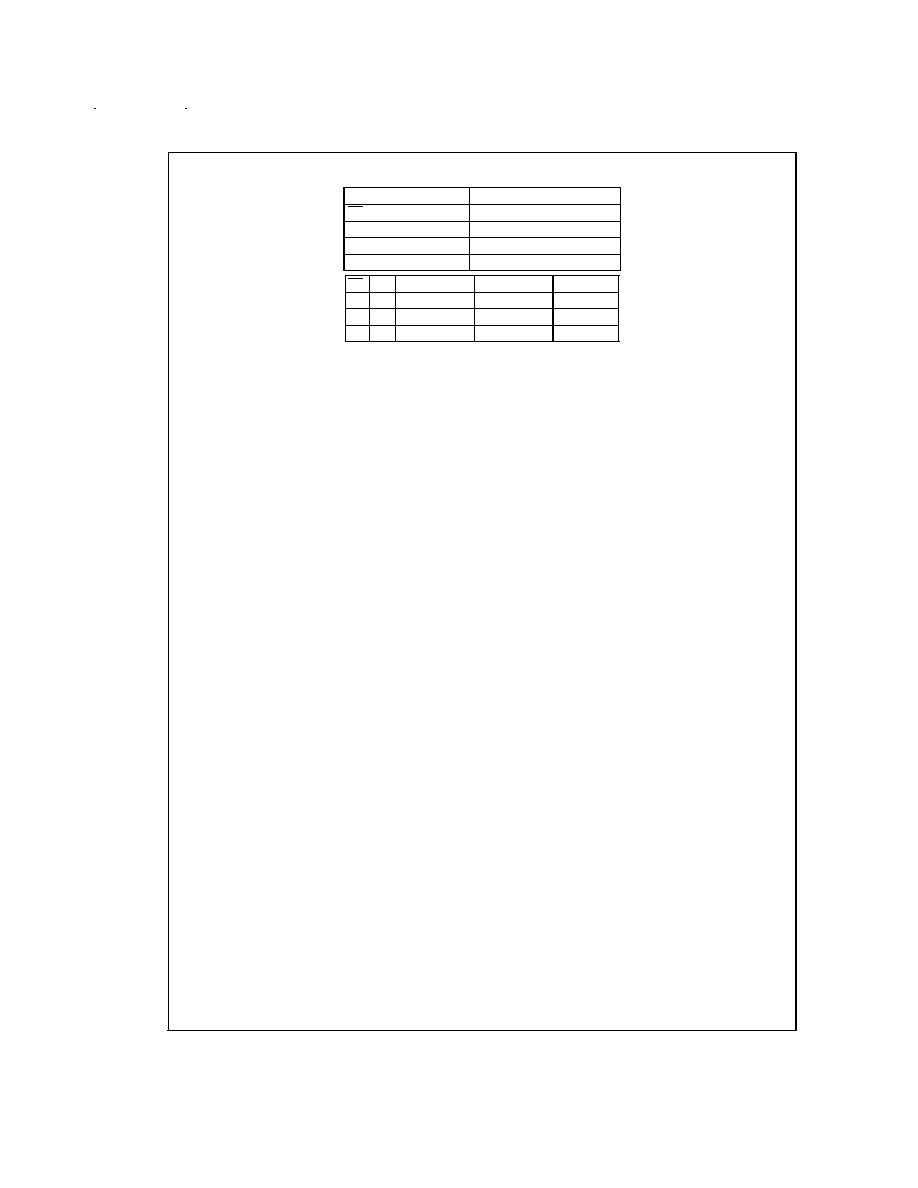
Pin Descriptions
Pin Names
Description
BE
Bus Switch Enable
BX
Bus Exchange
A
0
≠A
4
, B
0
≠B
4
Buses A, B
C
0
≠C
4
, D
0
≠D
4
Buses C, D
BE
BX
A
0
≠A
4
B
0
≠B
4
Function
H
X
High-Z State
High-Z State
Disconnect
L
L
C
0
≠C
4
D
0
≠ D
4
Connect
L
H
D
0
≠D
4
C
0
≠C
4
Exchange
www.national.com
2

Absolute Maximum Ratings
(Note 1)
If Military/Aerospace specified devices are required,
please contact the National Semiconductor Sales Office/
Distributors for availability and specifications.
Supply Voltage (V
CC
)
-0.5V to +7.0V
DC Switch Voltage (V
S
)
-0.5V to +7.0V
DC Input Voltage (V
I
) (Note 2)
-0.5V to +7.0V
DC Input Diode Current (I
IN
)
with V
I
<
0
-20 mA
DC Output (I
O
) Sink Current
30 mA
Storage Temperature Range (T
STG
)
-65∞C to +150∞C
Junction Temperature (T
J
)
175∞C
Power Dissipation
500mW
Recommended Operating
Conditions
Supply Voltage (V
CC
)
4.5V to 5.5V
Input Voltage (V
IN
)
0V to 5.5V
Input Rise and Fall Time (tr, t
f
)
Switch Control Input
0ns/V to 8ns/V
Switch I/O
0ns/V to DC
Free Air Operating Temperature (T
A
)
-55∞C to +125∞C
Note 1: The "Absolute Maximum Ratings" are those values beyond which
the safety of the device cannot be guaranteed. The device should not be op-
erated at these limits. The parametric values defined in the Electrical Charac-
teristics tables are not guaranteed at the absolute maximum ratings. The
"Recommended Operating Conditions" table will define the conditions for ac-
tual device operation.
Note 2: The input and output negative voltage ratings may be exceeded if
the input and output diode current ratings are observed.
DC Electrical Characteristics
Symbol
Parameter
V
CC
(V)
T
A
= -55∞C to
+125∞C
Units
Conditions
Min
Max
V
IK
Maximum Clamp
4.5
-1.2
V
I
IN
= -18 mA
Diode Voltage
V
IH
Minimum High
4.5≠5.5
2.0
V
Level Input Voltage
V
IL
Maximum Low
4.5≠5.5
0.8
Level Input Voltage
I
IN
Maximum Input
0
10
µA
0
V
IN
5.5V
Leakage Current
5.5
±
1
I
OZ
Maximum TRI-STATE
5.5
±
10
µA
0
A, B
V
CC
I/O Leakage
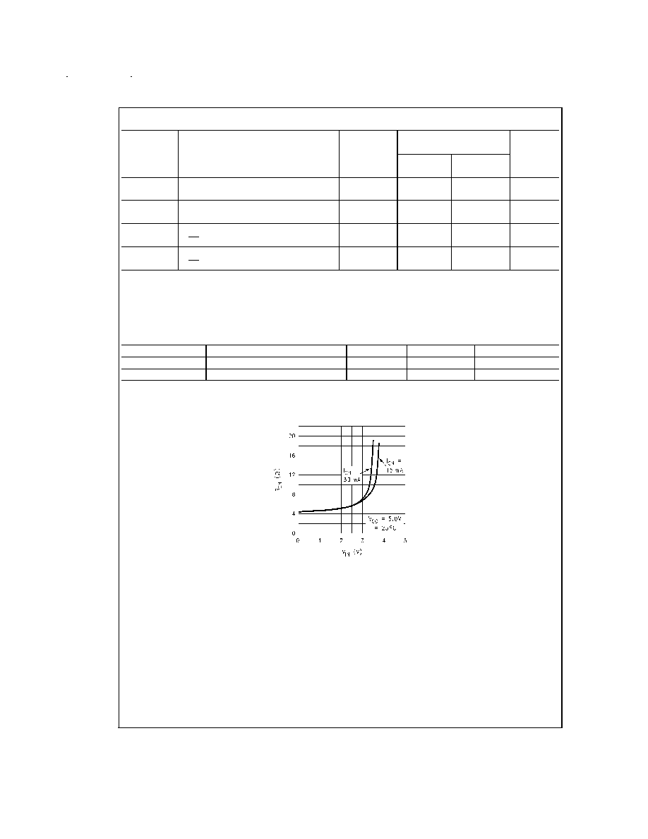
R
ON
Switch On
4.5
10
V
I
= 0V, I
ON
= 30 mA
Resistance (Note 3)
20
V
I
= 2.4V, I
ON
= 15 mA
I
CC
Maximum Quiescent
5.5
10
µA
V
I
= V
CC
, GND
Supply Current
I
O
= 0
I
CC
Increase in I
CC
5.5
2.5
mA
V
IN
= 3.15V, I
O
= 0
per Input (Note 4)
Per Control Input
Note 3: Measured by voltage drop between A and B pin at indicated current through the switch. On resistance is determined by the lower of the voltages on the two
(A or B) pins.
Note 4: Per TTL driven input (V
IN
= 3.15V, control inputs only). A and B pins do not contribute to I
CC
.
www.national.com
3
AC Electrical Characteristics
Symbol
Parameter
V
CC
(V)
T
A
= -55∞C to +125∞C
Units
C
L
= 50 pF
Min
Max
t
PLH
,
Data Propagation Delay
4.5-5.5
0.25
ns
t
PHL
A
n
to C
n
, D
n
or B
n
to D
n
, C
n
(Note 6)
t
PLH
,
Switch Exchange Time
4.5-5.5
1.5
7.0
ns
t
PHL
BX to A
n
, B
n
, C
n
, D
n
t
PZL
,
Switch Enable Time
4.5-5.5
1.5
7.0
ns
t
PZH
BE to A
n
, B
n
, C
n
or D
n
t
PLZ
,
Switch Disable Time
4.5-5.5
1.5
7.0
ns
t
PHZ
BE to A
n
, B
n
, C
n
, or D
n
Note 5: All typical values are at V
CC
= 5.0V, T
A
= 25∞C.
Note 6: This parameter is guaranteed by design but not tested. The bus switch contributes no propagation delay other than the RC delay of the On resistance of
the switch and the load capacitance. The time constant for the switch and alone is of the order of 0.25 ns for 50 pF load. Since this time constant is much smaller
than the rise/fall times of typical driving signals, it adds very little propagation delay to the system. Propagation delay of the bus switch when used in a system is de-
termined by the driving circuit on the driving side of the switch and its interaction with the load on the driven side.
Capacitance
(Note 7)
Symbol
Parameter
Max
Units
Conditions
C
IN
Control Input Capacitance
12
pF
V
CC
= 5.0V
C
I/O
(OFF)
Input/Output Capacitance
20
pF
V
CC
= 5.0V
Note 7: Capacitance is characterized but not tested.
54LVX3383 V
IN
vs R
ON
(Typ)
DS011652-4
www.national.com
4
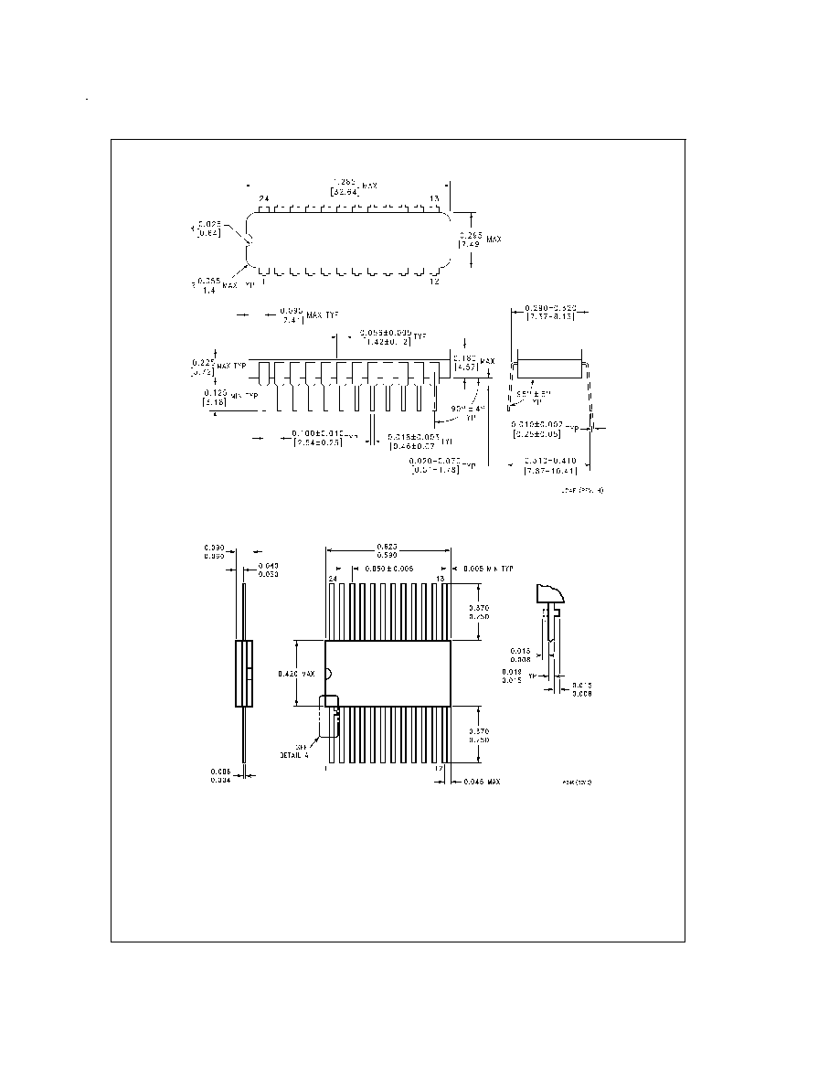
Physical Dimensions
inches (millimeters) unless otherwise noted
24-Lead Ceramic Dual-in-line
Package Number J24F
24-Lead Cerpack
Package Number W24C
www.national.com
5