54LVX3384
10-Bit Low Power Bus Switch
General Description
The 54LVX3384 provides 10 bits of high-speed CMOS
TTL-compatible bus switches. The low on resistance of the
switch allows inputs to be connected to outputs without add-
ing propagation delay or generating additional ground
bounce noise. The device is organized as two 5-bit switches
with separate bus enable (OE ) signals. When OE is low, the
switch is on and port A is connected to port B. When OE is
high, the switch is open and a high-impedance state exists
between the two ports.
Features
n
4
switch connection between two ports
n
Minimal propagation delay through the switch
n
Ultra low power with
<
0.1 µA typical I
CC
n
Zero ground bounce in flow-through mode
n
Control inputs compatible with TTL levels
n
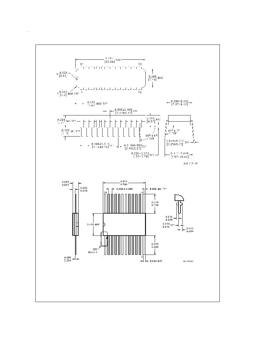
Available in CDIP and Cerpack Packaging
n
Standard Microcircuit Drawing (SMD) 5962-9950701
Ordering Code
Order Number
Package Number
Package Description
54LVX3384J-QML
J24F
24-Lead Ceramic Dual-in-line
54LVX3384W-QML
W24C
24-Lead Cerpack
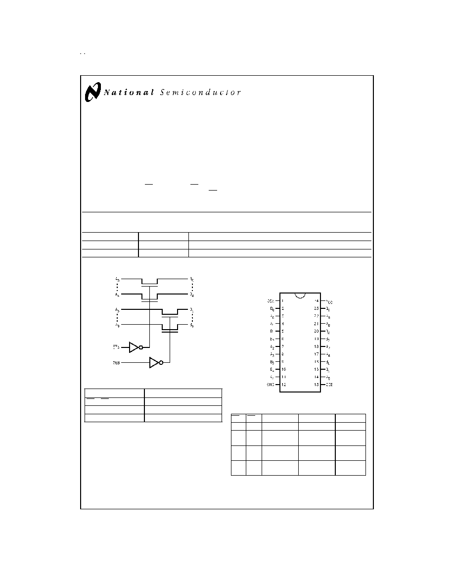
Logic Diagram
Pin Descriptions
Pin Names
Description
OEA, OEB
Bus Switch Enable
A
0
≠A
9
Bus A
B
0
≠B
9
Bus B
Connection Diagram
Truth Table
OEA OEB
B
0
≠B
4
B
5
≠B
9
Function
L
L
A
0
≠A
4
A
5
≠A
9
Connect
L
H
A
0
≠A
4
HIGH-Z
State
Connect
H
L
HIGH-Z
State
A
5
≠A
9
Connect
H
H
HIGH-Z
State
HIGH-Z
State
Disconnect
DS101061-1
Pin Assignment for
CDIP and Cerpack
DS101061-2
April 1999
54L
VX3384
10-Bit
Low
Power
Bus
Switch
© 1999 National Semiconductor Corporation
DS101061
www.national.com
Absolute Maximum Ratings
(Note 1)
If Military/Aerospace specified devices are required,
please contact the National Semiconductor Sales Office/
Distributors for availability and specifications.
Supply Voltage (V
CC
)
-0.5V to +7.0V
DC Switch Voltage (V
S
)
-0.5V to +7.0V
DC Input Voltage (V
IN
) (Note 2)
-0.5V to +7.0V
DC Input Diode Current (I
IK
) V
IN
<
0V
-20 mA
DC Output (I
OUT
) Sink Current
100 mA
Storage Temperature Range (T
STG
)
-65∞C to +150∞C
Power Dissapation
500mW
Junction Temperature (T
J
)
175∞C
Recommended Operating
Conditions
(Note 3)
Power Supply Operating (V
CC
)
4.5V to 5.5V
Input Voltage (V
IN
)
0V to 5.5V
Input Rise and Fall Time (t
r
, t
f
)
Switch Control Input
0nS/V to 5nS/V
Switch I/O
0nS/V to DC
Free Air Operating Temperature (T
A
)
-55∞C to +125∞C
Note 1: The "Absolute Maximum Ratings" are those values beyond which
the safety of the device cannot be guaranteed. The device should not be op-
erated at these limits. The parametric values defined in the "Electrical Char-
acteristics" table are not guaranteed at the absolute maximum ratings. The
"Recommended Operating Conditions" table will define the conditions for ac-
tual device operation.
Note 2: The input and output negative voltage ratings may be exceeded if
the input and output diode current ratings are observed.
Note 3: Unused control inputs must be held HIGH or LOW. They may not
float.
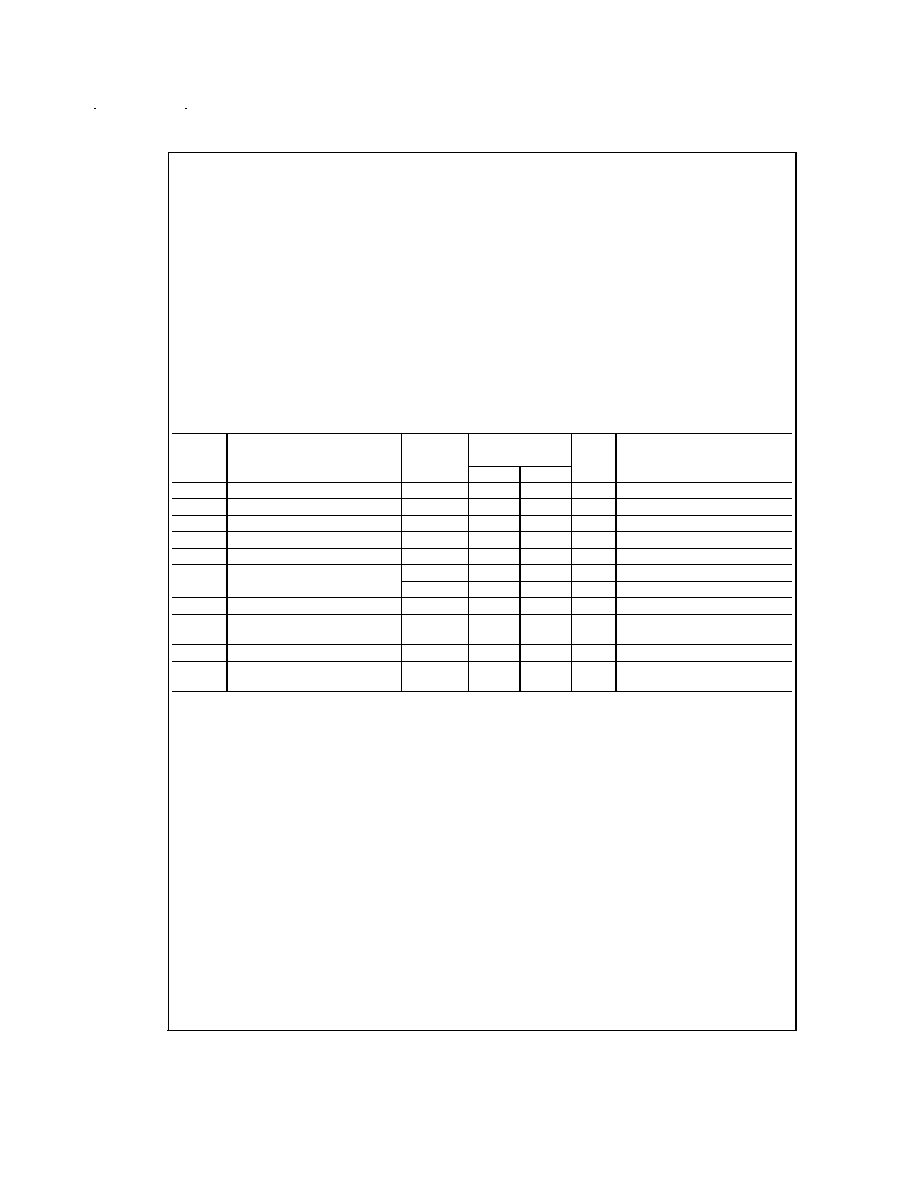
DC Electrical Characteristics
Symbol
Parameter
V
CC
(V)
T
A
= -55∞C to
+125∞C
Units
Condition
Min
Max
V
IC
Clamp Diode Voltage
4.5
-1.2
V
I
IN
= - 18mA
V
IH
High Level Input Voltage
4.5-5.5
2.0
V
V
IL
Low Level Input Voltage
4.5-5.5
0.8
V
I
I
Input Leakage Current
5.5
±
1.0
µA
0
V
IN
5.5V
I
OZ
TRI-STATE Leakage Current
5.5
±
10.0
µA
0
A, B
V
CC
R
ON
Switch On Resistance
(Note 4)
4.5
10
V
IN
= 0V, I
IN
= 30mA
4.5
20
V
IN
= 0V, I
IN
= 15mA
I
CC
Quiescent Supply Current
5.5
10
µA
V
IN
= V
CC
or GND, I
OUT
= 0
I
CC
Increase in I
cc
per Input
5.5
2.5
mA
One input at 3.4V
Other inputs at V
CC
or GND
I
OFF
Power Off Leakage Current
0.0
10
µA
V
IN
= 5.5V or 0.0V
I
OS
Short Circuit Output Current
(Note 5)
4.5
80
mA
V
IN
= 4.5V, V
OUT
= 0.0V
Note 4: Measured by voltage drop between A and B pin at indicated current through the switch. On resistance is determined by the lower of the voltages on the two
(A or B) pins.
Note 5: Not more than one output tested at a time.
www.national.com
2
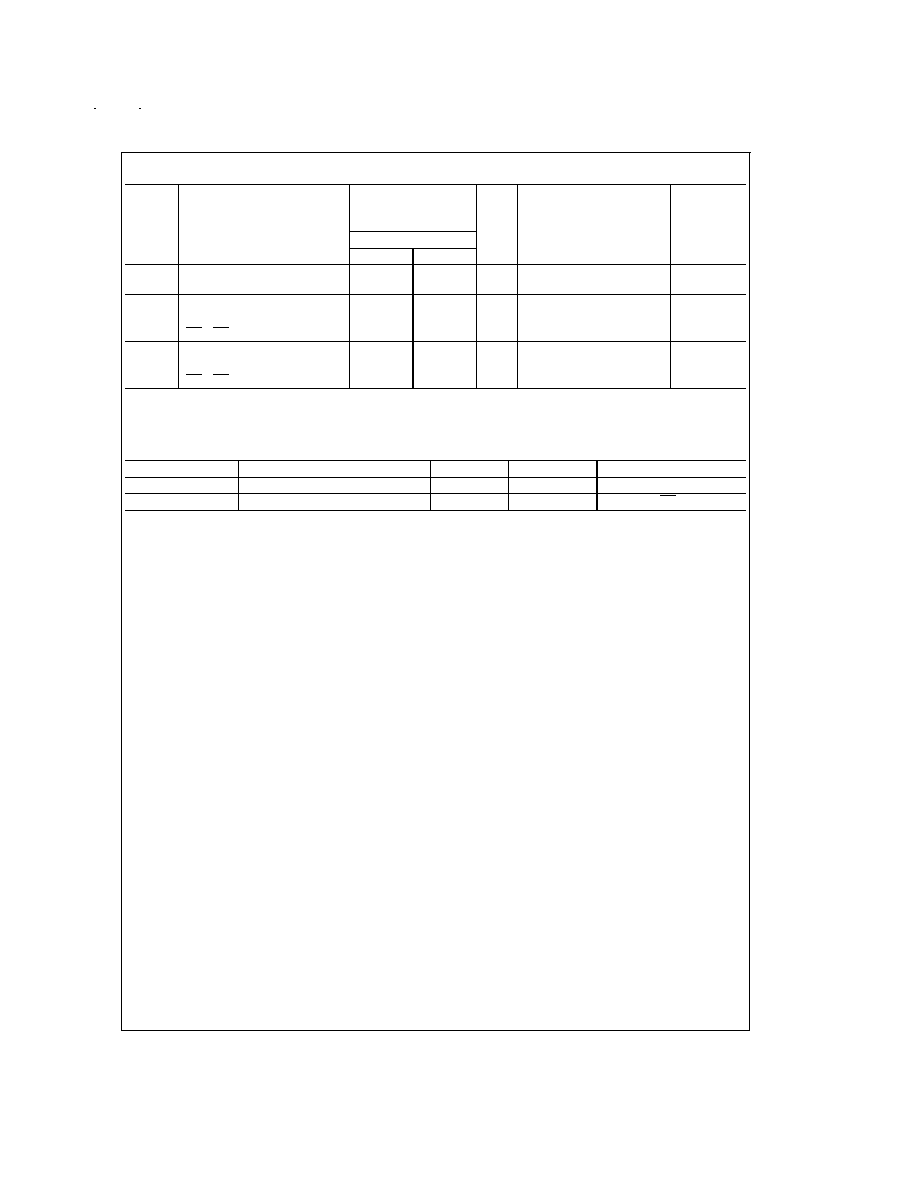
AC Electrical Characteristics
Symbol
Parameter
T
A
= -55∞C to +125∞C
C
L
= 50 pF,
RU=RD=500
Units
Conditions
Figure No.
V
CC
= 4.5 - 5.5V
Min
Max
t
PHL
,
t
PLH
Prop Delay Bus to Bus (Note 6)
0.25
ns
V
I
= open
Figures 1, 2
t
PZH
,
t
PZL
Output Enable Time
1.0
6.0
ns
V
I
= 7V for t
PZL
Figures 1, 2
OE
A
, OE
B
to An, Bn
V
I
= open for t
PZH
t
PHZ
,
t
PLZ
Output Disable Time
1.0
6.0
ns
I
I
= 7V for t
PLZ
Figures 1, 2
OE
A
, OE
B
to An, Bn
V
I
= open for t
PHZ
Note 6: This parameter is guaranteed by design but not tested. The bus switch contributes no propagation delay other than the RC delay of the typical On resistance
of the switch and the 50pF load capacitance, when driven by an ideal voltage the source (zero output impedance).
Capacitance
(Note 7)
Symbol
Parameter
Max
Units
Conditions
C
IN
Control Input Capacitance
10
pF
V
CC
= Open
C
I/O
(OFF)
Input/Output Capacitance
12
pF
V
CC
, OE = 5.0V
Note 7: Capacitance is characterized but not tested.
www.national.com
3
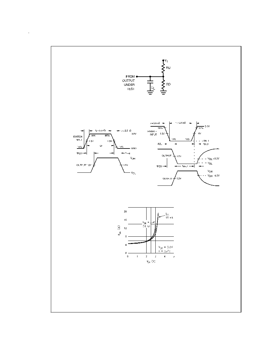
AC Loading and Waveforms
DS101061-4
Note: Input driven by 50 Ohms source terminated in 50 Ohms
Note: C
L
includes load and stray capacitance
Note: Input PRR=1.0 MHz, t
W
= 500 nS
FIGURE 1. AC Test Circuit
DS101061-5
FIGURE 2. AC Waveforms
54LVX3384 V
IN
vs R
ON
(Typ)
DS101061-3
www.national.com
4