LP2950/LP2951
Series of Adjustable Micropower Voltage Regulators
General Description
The LP2950 and LP2951 are micropower voltage regulators
with very low quiescent current (75µA typ.) and very low
dropout voltage (typ. 40mV at light loads and 380mV at
100mA). They are ideally suited for use in battery-powered
systems. Furthermore, the quiescent current of the LP2950/
LP2951 increases only slightly in dropout, prolonging battery
life.
The LP2950-5.0 is available in the surface-mount D-Pak
package, and in the popular 3-pin TO-92 package for pin-
compatibility with older 5V regulators. The 8-lead LP2951 is
available in plastic, ceramic dual-in-line, or metal can pack-
ages and offers additional system functions.
One such feature is an error flag output which warns of a low
output voltage, often due to falling batteries on the input. It
may be used for a power-on reset. A second feature is the
logic-compatible shutdown input which enables the regulator
to be switched on and off. Also, the part may be pin-strapped
for a 5V, 3V, or 3.3V output (depending on the version), or
programmed from 1.24V to 29V with an external pair of
resistors.
Careful design of the LP2950/LP2951 has minimized all
contributions to the error budget. This includes a tight initial
tolerance (.5% typ.), extremely good load and line regulation
(.05% typ.) and a very low output voltage temperature coef-
ficient, making the part useful as a low-power voltage refer-
ence.
Features
n
5V, 3V, and 3.3V versions available
n
High accuracy output voltage
n
Guaranteed 100mA output current
n
Extremely low quiescent current
n
Low dropout voltage
n
Extremely tight load and line regulation
n
Very low temperature coefficient
n
Use as Regulator or Reference
n
Needs minimum capacitance for stability
n
Current and Thermal Limiting
n
Stable with low-ESR output capacitors
LP2951 versions only
n
Error flag warns of output dropout
n
Logic-controlled electronic shutdown
n
Output programmable from 1.24 to 29V
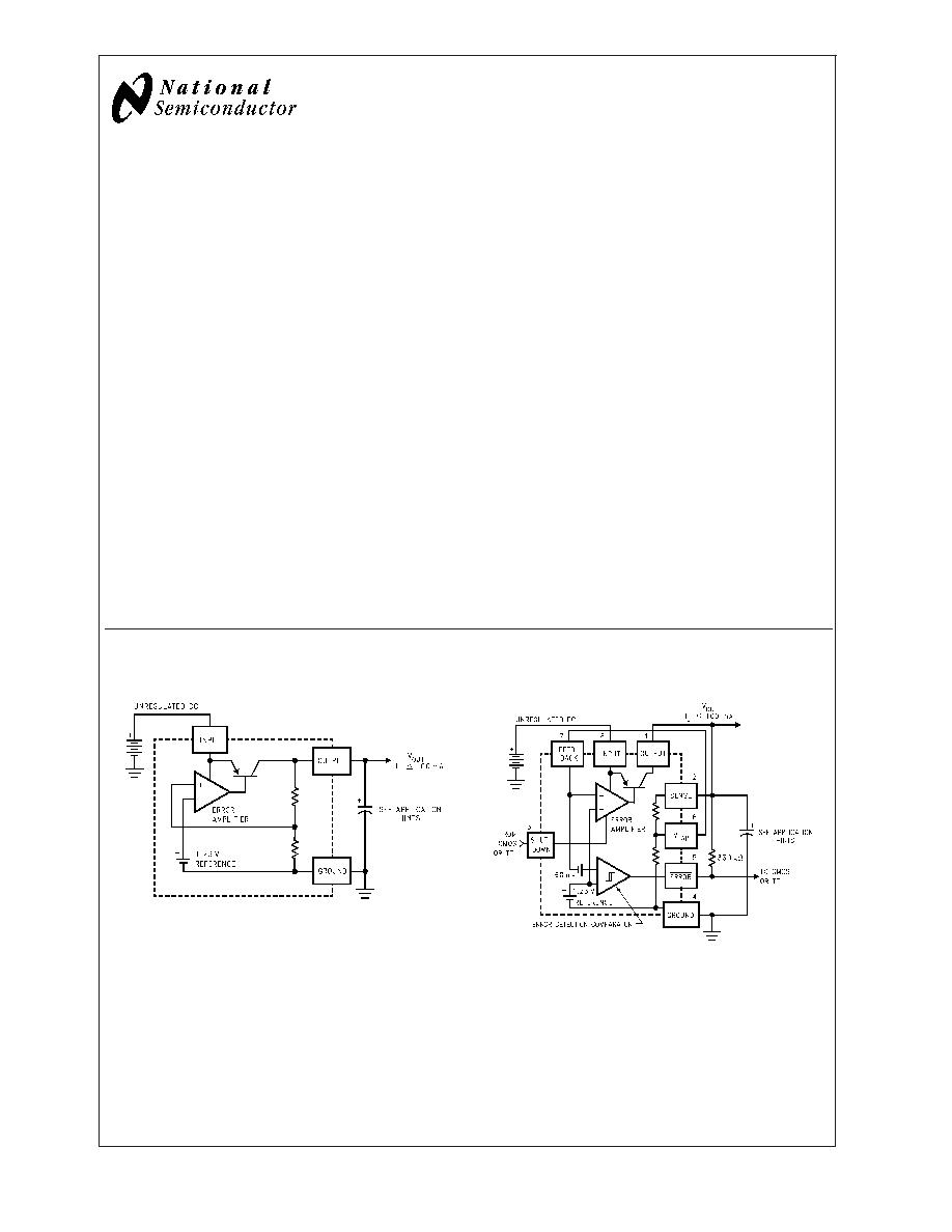
Block Diagram and Typical Applications
LP2950
LP2951
00854625
00854601
May 2003
LP2950/LP2951
Series
of
Adjustable
Micropower
V
oltage
Regulators
© 2003 National Semiconductor Corporation
DS008546
www.national.com
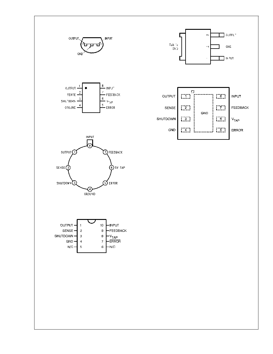
Connection Diagrams
TO-92 Plastic Package (Z)
00854602
Bottom View
Dual-In-Line Packages (N, J)
Surface-Mount Package (M, MM)
00854626
Top View
Metal Can Package (H)
00854619
Top View
10-Lead Ceramic Surface-Mount Package (WG)
00854664
Top View
TO-252 (D-Pak)
00854670
Front View
8-Lead LLP
00854671
Pin 4 is fused to center DAP
Top View
LP2950/LP2951
www.national.com
2
Absolute Maximum Ratings
(Note 1)
If Military/Aerospace specified devices are required,
please contact the National Semiconductor Sales Office/
Distributors for availability and specifications.
Input Supply Voltage
-0.3 to +30V
SHUTDOWN Input Voltage,
Error Comparator Output
Voltage, (Note 9)
FEEDBACK Input Voltage
-1.5 to +30V
(Note 9) (Note 10)
Power Dissipation
Internally Limited
Junction Temperature (T
J
)
+150∞C
Ambient Storage Temperature
-65∞ to +150∞C
Soldering Dwell Time, Temperature
Wave
Infrared
Vapor Phase
4 seconds, 260∞C
10 seconds, 240∞C
75 seconds, 219∞C
ESD Rating
Human Body Model(Note 18)
2500V
Operating Ratings
(Note 1)
Maximum Input Supply Voltage
30V
Junction Temperature Range
(T
J
) (Note 8)
LP2951
-55∞ to +150∞C
LP2950AC-XX, LP2950C-XX,
LP2951AC-XX, LP2951C-XX
-40∞ to +125∞C
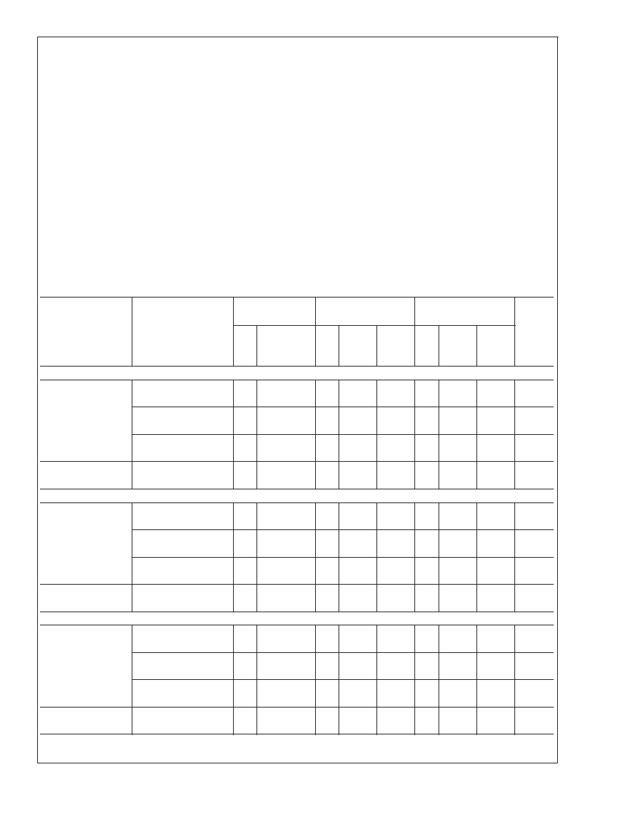
Electrical Characteristics
(Note 2)
Parameter
Conditions
(Note 2)
LP2951
LP2950AC-XX
LP2950C-XX
Units
LP2951AC-XX
LP2951C-XX
Tested
Tested
Design
Tested
Design
Typ
Limit
Typ
Limit
Limit
Typ
Limit
Limit
(Notes 3, 16)
(Note 3) (Note 4)
(Note 3) (Note 4)
3V Versions (Note 17)
Output Voltage
T
J
= 25∞C
3.0
3.015
3.0
3.015
3.0
3.030
V max
2.985
2.985
2.970
V min
-25∞C
T
J
85∞C
3.0
3.0
3.030
3.0
3.045
V max
2.970
2.955
V min
Full Operating
3.0
3.036
3.0
3.036
3.0
3.060
V max
Temperature Range
2.964
2.964
2.940
V min
Output Voltage
100µA
I
L
100mA
3.0
3.045
3.0
3.042
3.0
3.072
V max
T
J
T
JMAX
2.955
2.958
2.928
V min
3.3V Versions (Note 17)
Output Voltage
T
J
= 25∞C
3.3
3.317
3.3
3.317
3.3
3.333
V max
3.284
3.284
3.267
V min
-25∞C
T
J
85∞C
3.3
3.3
3.333
3.3
3.350
V max
3.267
3.251
V min
Full Operating
3.3
3.340
3.3
3.340
3.3
3.366
V max
Temperature Range
3.260
3.260
3.234
V min
Output Voltage
100µA
I
L
100mA
3.3
3.350
3.3
3.346
3.3
3.379
V max
T
J
T
JMAX
3.251
3.254
3.221
V min
5V Versions (Note 17)
Output Voltage
T
J
= 25∞C
5.0
5.025
5.0
5.025
5.0
5.05
V max
4.975
4.975
4.95
V min
-25∞C
T
J
85∞C
5.0
5.0
5.05
5.0
5.075
V max
4.95
4.925
V min
Full Operating
5.0
5.06
5.0
5.06
5.0
5.1
V max
Temperature Range
4.94
4.94
4.9
V min
Output Voltage
100µA
I
L
100mA
5.0
5.075
5.0
5.075
5.0
5.12
V max
T
J
T
JMAX
4.925
4.925
4.88
V min
LP2950/LP2951
www.national.com
5