
DS26LS32AC/DS26LS32C/DS26LS32M/DS26LS33M
Quad Differential Line Receivers
General Description
The DS26LS32 and DS26LS32A are quad differential line re-
ceivers designed to meet the RS-422, RS-423 and Federal
Standards 1020 and 1030 for balanced and unbalanced digi-
tal data transmission.
The DS26LS32 and DS26LS32A have an input sensitivity of
200 mV over the input voltage range of
±
7V and the
DS26LS33 have an input sensitivity of 500 mV over the input
voltage range of
±
15V.
The DS26LS32A differ in function from the popular
DS26LS32 and DS26LS33 in that input pull-up and
pull-down resistors are included which prevent output oscil-
lation on unused channels.
Each version provides an enable and disable function com-
mon to all four receivers and features TRI-STATE
Æ
outputs
with 8 mA sink capability. Constructed using low power
Schottky processing, these devices are available over the
full military and commerical operating temperature ranges.
Features
n
High differential or common-mode input voltage ranges
of
±
7V on the DS26LS32 and DS26LS32A and
±
15V
on the DS26LS33
n
±
0.2V sensitivity over the input voltage range on the
DS26LS32 and DS26LS32A,
±
0.5V sensitivity on the
DS26LS33
n
DS26LS32 and DS26LS32A meet all requirements of
RS-422 and RS-423
n
6k minimum input impedance
n
100 mV input hysteresis on the DS26LS32 and
DS26LS32A, 200 mV on the DS26LS33
n
Operation from a single 5V supply
n
TRI-STATE outputs, with choice of complementary
output enables for receiving directly onto a data bus
Logic Diagram
TRI-STATE
Æ
is a registered trademark of National Semiconductor Corporation.
DS005255-1
May 1999
DS26LS32AC/DS26LS32C/DS26LS32M/DS26LS33MQuad
Differential
Line
Receivers
© 1999 National Semiconductor Corporation
DS005255
www.national.com

Connection Diagram
Truth Table
ENABLE
ENABLE
Input
Output
0
1
X
Hi-Z
See
V
ID
V
TH
(Max)
1
Note Below
V
ID
V
TH
(Min)
0
Hi-Z = TRI-STATE
Æ
Note: Input conditions may be any combination not defined for ENABLE and ENABLE .
Dual-In-Line Package
DS005255-2
Top View
Order Number DS26LS32CM, DS26LS32CN,
DS26LS32ACM, DS26LS32ACN, DS26LS33ACM
or DS26LS33ACN
See NS Package Number M16A or N16E
For Complete Military Product Specifications,
refer to the appropriate SMD or MDS.
Order Number DS26LS32MJ/883, DS26LS32MW/883,
DS26LS32ME/883, DS26LS33MW/883
See NS Package Number E20A, J16A or W16A
20-Lead Ceramic Leadless Chip Carrier
DS005255-12
www.national.com
2

Absolute Maximum Ratings
(Note 3)
If Military/Aerospace specified devices are required,
please contact the National Semiconductor Sales Office/
Distributors for availability and specifications.
Supply Voltage
7V
Common-Mode Range
±
25V
Differential Input Voltage
±
25V
Enable Voltage
7V
Output Sink Current
50 mA
Maximum Power Dissipation (Note 1) at 25∞C
Cavity Package
1433 mW
Molded Dip Package
1362 mW
SO Package DS26LS32
1002 mW
DS26LS32A
1051 mW
Storage Temperature Range
-65∞C to
+165∞C
Lead Temperature (Soldering, 4 seconds)
260∞C
Operating Conditions
Min
Max
Units
Supply Voltage, (V
CC
)
DS26LS32M, DS26LS33M
4.5
5.5
V
(MIL)
DS26LS32C
4.75
5.25
V
DS26LS32AC
(COML)
Temperature, (T
A
)
DS26LS32M, DS26LS33M
-55
+125
∞C
(MIL)
DS26LS32C
0
+70
∞C
DS26LS32AC
(COML)
Note 1: Derate cavity package 9.6 mW/∞C above 25∞C; derate molded DIP
package 10.9 mW/∞C above 25∞C.
Note 2: Derate SO Package 8.01 mW/∞C for DS26LS32
8.41 mW/∞C for DS26LS32A
Electrical Characteristics
(Notes 4, 5, 6)
over the operating temperature range unless otherwise specified
Symbol
Parameter
Conditions
Min
Typ
Max
Units
V
TH
Differential Input
V
OUT
= V
OH
DS26LS32, DS26LS32A, -7V
V
CM
+7V
-0.2
±
0.07
0.2
V
Voltage
or V
OL
DS26LS33, DS26LS33A, -15V
V
CM
+15V
-0.5
±
0.14
0.5
V
R
IN
Input Resistance
-15V
V
CM
+15V (One Input AC GND)
6.0
8.5
k
I
IN
Input Current (Under
V
IN
= 15V, Other Input -15V
V
IN
+15V
2.3
mA
Test)
V
IN
= -15V, Other Input -15V
V
IN
+15V
-2.8
mA
V
OH
Output High Voltage
V
CC
= MIN,
V
IN
= 1V,
Commercial
2.7
4.2
V
V
ENABLE
= 0.8V, I
OH
= -440 µA
Military
2.5
4.2
V
V
OL
Output Low Voltage
V
CC
= Min,
V
IN
= -1V,
I
OL
= 4 mA
0.4
V
V
ENABLE
= 0.8V
I
OL
= 8 mA
0.45
V
V
IL
Enable Low Voltage
0.8
V
V
IH
Enable High Voltage
2.0
V
V
I
Enable Clamp
V
CC
= Min, I
IN
= -18 mA
-1.5
V
Voltage
I
O
OFF-State (High
V
CC
= Max
V
O
= 2.4V
20
µA
Impedance) Output
V
O
= 0.4V
-20
µA
Current
I
IL
Enable Low Current
V
IN
= 0.4V
-0.36
mA
I
IH
Enable High Current
V
IN
= 2.7V
20
µA
I
SC
Output Short-Circuit
V
O
= 0V, V
CC
= Max,
V
IN
= 1V
-15
-85
mA
Current
I
CC
Power Supply
V
CC
= Max, All V
IN
= GND,
DS26LS32, DS26LS32A
52
70
mA
Current
Outputs Disabled
DS26LS33, DS26LS33A
57
80
mA
I
I
Input High Current
V
IN
= 5.5V
100
µA
V
HYST
Input Hysteresis
T
A
= 25∞C, V
CC
= 5V,
DS26LS32, DS26S32A
100
mV
V
CM
= 0V
DS26LS33, DS26LS33A
200
mV
Note 3: "Absolute Maximum Ratings" are those values beyond which the safety of the device cannot be guaranteed. They are not meant to imply that the device
should be operated at these limits. The table of "Electrical Characteristics" provides conditions for actual device operation.
Note 4: All currents into device pins are shown as positive, all currents out of device pins are shown as negative, all voltages are referenced to ground, unless oth-
erwise specified. All values shown as max or min are so classified on absolute value basis.
Note 5: All typical values are V
CC
= 5V, T
A
= 25∞C.
Note 6: Only one output at a time should be shorted.
www.national.com
3
Switching Characteristics
V
CC
= 5V, T
A
= 25∞C
Symbol
Parameter
Conditions
DS26LS32/DS26LS33
DS26LS32A/DS26LS33A
Units
Min
Typ
Max
Min
Typ
Max
t
PLH
Input to Output
C
L
= 15 pF
17
25
23
35
ns
t
PHL
17
25
23
35
ns
t
LZ
ENABLE to Output
C
L
= 5 pF
20
30
15
30
ns
t
HZ
15
22
20
25
ns
t
ZL
ENABLE to Output
C
L
= 15 pF
15
22
14
22
ns
t
ZH
15
22
15
22
ns
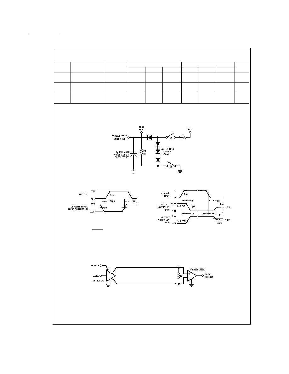
AC Test Circuit and Switching Time Waveforms
Typical Applications
Load Test Circuit for TRI-STATE
Æ
Outputs
DS005255-3
Propagation Delay (Notes 7, 9)
DS005255-4
Enable and Disable Times (Notes 8, 9)
DS005255-5
Note 7: Diagram shown for ENABLE low.
Note 8: S1 and S2 of load circuit are closed except where shown.
Note 9: Pulse generator for all pulses: Rate = 1.0 MHz; Z
O
= 50
; t
r
6 ns; t
f
6.0 ns.
Two-Wire Balanced Interface -- RS-422
DS005255-6
www.national.com
4
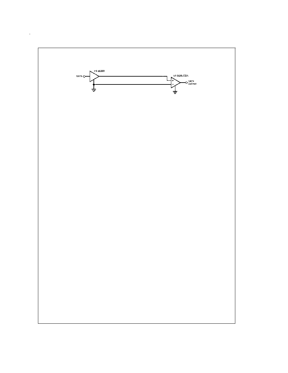
Typical Applications
(Continued)
Single Wire with Driver Ground Reference -- RS-423
DS005255-7
www.national.com
5