LM78S40 Universal Switching Regulator Subsystem
LM78S40
Universal Switching Regulator Subsystem
General Description
The LM78S40 is a monolithic regulator subsystem consisting
of all the active building blocks necessary for switching regu-
lator systems. The device consists of a temperature com-
pensated voltage reference, a duty-cycle controllable oscilla-
tor with an active current limit circuit, an error amplifier, high
current, high voltage output switch, a power diode and an
uncommitted operational amplifier. The device can drive ex-
ternal NPN or PNP transistors when currents in excess of
1.5A or voltages in excess of 40V are required. The device
can be used for step-down, step-up or inverting switching
regulators as well as for series pass regulators. It features
wide supply voltage range, low standby power dissipation,
high efficiency and low drift. It is useful for any stand-alone,
low part count switching system and works extremely well in
battery operated systems.
Features
n
Step-up, step-down or inverting switching regulators
n
Output adjustable from 1.25V to 40V
n
Peak currents to 1.5A without external transistors
n
Operation from 2.5V to 40V input
n
Low standby current drain
n
80 dB line and load regulation
n
High gain, high current, independent op amp
n
Pulse width modulation with no double pulsing
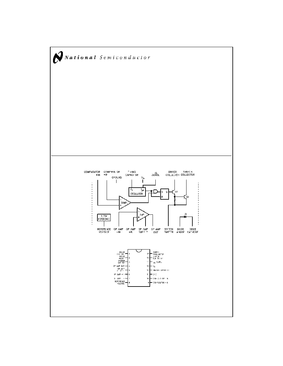
Block and Connection Diagrams
DS010057-2
16-Lead DIP
DS010057-1
Top View
April 1998
LM78S40
Universal
Switching
Regulator
Subsystem
© 1998 National Semiconductor Corporation
DS010057
www.national.com
Ordering Information
Part Number
NS Package
Temperature Range
LM78S40J/883
J16A Ceramic DIP
-55°C to +125°C
LM78S40N
N16E Molded DIP
-40°C to +125°C
LM78S40CN
N16E Molded DIP
0°C to +70°C
www.national.com
2
Absolute Maximum Ratings
(Note 1)
If Military/Aerospace specified devices are required,
please contact the National Semiconductor Sales Office/
Distributors for availability and specifications.
Storage Temperature Range
Ceramic DIP
-65°C to +175°C
Molded DIP
-65°C to +150°C
Operating Temperature Range
Extended (LM78S40J)
-55°C to +125°C
Industrial (LM78S40N)
-40°C to +125°C
Commercial (LM78S40CN)
0°C to +70°C
Lead Temperature
Ceramic DIP (Soldering, 60 sec.)
300°C
Molded DIP (Soldering, 10 sec.)
265°C
Internal Power Dissipation (Note 2) (Note 3)
16L-Ceramic DIP
1.50W
16L-Molded DIP
1.04W
Input Voltage from V
IN
to GND
40V
Input Voltage from V
+
(Op Amp)
to GND
40V
Common Mode Input Range
(Comparator and Op Amp)
-0.3 to V+
Differential Input Voltage
(Note 4)
±
30V
Output Short Circuit
Duration (Op Amp)
Continuous
Current from V
REF
10 mA
Voltage from Switch
Collectors to GND
40V
Voltage from Switch
Emitters to GND
40V
Voltage from Switch
Collectors to Emitter
40V
Voltage from Power Diode to GND
40V
Reverse Power Diode Voltage
40V
Current through Power Switch
1.5A
Current through Power Diode
1.5A
ESD Susceptibility
(to be determined)
LM78S40
Electrical Characteristics
(Note 5)
T
A
= Operating temperature range, V
IN
= 5.0V, V
+
(Op Amp) = 5.0V, unless otherwise specified.
Symbol
Parameter
Conditions
Min
Typ
Max
Units
GENERAL CHARACTERISTICS
I
CC
Supply Current
V
IN
= 5.0V
1.8
3.5
mA
(Op Amp Disconnected)
V
IN
= 40V
2.3
5.0
mA
I
CC
Supply Current
V
IN
= 5.0V
4.0
mA
(Op Amp Connected)
V
IN
= 40V
5.5
mA
REFERENCE SECTION
V
REF
Reference Voltage
I
REF
= 1.0 mA
Extend -55°C
<
T
A
<
+125°C,
Comm 0
<
T
A
<
+70°C,
1.180
1.245
1.310
V
Indus -40°C
<
T
A
<
+85°C
V
R LINE
Reference Voltage
V
IN
= 3.0V to V
IN
= 40V,
0.04
0.2
mV/V
Line Regulation
I
REF
= 1.0 mA, T
A
= 25°C
V
R LOAD
Reference Voltage
I
REF
= 1.0 mA to I
REF
= 10 mA,
0.2
0.5
mV/mA
Load Regulation
T
A
= 25°C
OSCILLATOR SECTION
I
CHG
Charging Current
V
IN
= 5.0V, T
A
= 25°C
20
50
µA
I
CHG
Charging Current
V
IN
= 40V, T
A
= 25°C
20
70
µA
I
DISCHG
Discharge Current
V
IN
= 5.0V, T
A
= 25°C
150
250
µA
I
DISCHG
Discharge Current
V
IN
= 40V, T
A
= 25°C
150
350
µA
V
OSC
Oscillator Voltage Swing
V
IN
= 5.0V, T
A
= 25°C
0.5
V
t
on
/t
off
Ratio of Charge/
6.0
µs/µs
Discharge Time
CURRENT LIMIT SECTION
V
CLS
Current Limit Sense
Voltage
T
A
= 25°C
250
350
mV
OUTPUT SWITCH SECTION
V
SAT 1
Output Saturation Voltage 1
I
SW
= 1.0A (Figure 1)
1.1
1.3
V
V
SAT 2
Output Saturation Voltage 2
I
SW
= 1.0A (Figure 2)
0.45
0.7
V
3
www.national.com
LM78S40
Electrical Characteristics
(Note 5) (Continued)
T
A
= Operating temperature range, V
IN
= 5.0V, V
+
(Op Amp) = 5.0V, unless otherwise specified.
Symbol
Parameter
Conditions
Min
Typ
Max
Units
OUTPUT SWITCH SECTION
h
FE
Output Transistor Current
Gain
I
C
= 1.0A, V
CE
= 5.0V, T
A
= 25°C
70
I
L
Output Leakage Current
V
O
= 40V, T
A
= 25°C
10
nA
POWER DIODE
V
FD
Forward Voltage Drop
I
D
= 1.0A
1.25
1.5
V
I
DR
Diode Leakage Current
V
D
= 40V, T
A
= 25°C
10
nA
COMPARATOR
V
IO
Input Offset Voltage
V
CM
= V
REF
1.5
15
mV
I
IB
Input Bias Current
V
CM
= V
REF
35
200
nA
I
IO
Input Offset Current
V
CM
= V
REF
5.0
75
nA
V
CM
Common Mode Voltage
Range
T
A
= 25°C
0
V
IN
2
V
PSRR
Power Supply Rejection
Ratio
V
IN
= 3.0V to 40V, T
A
= 25°C
70
96
dB
OPERATIONAL AMPLIFIER
V
IO
Input Offset Voltage
V
CM
= 2.5V
4.0
15
mV
I
IB
Input Bias Current
V
CM
= 2.5V
30
200
nA
I
IO
Input Offset Current
V
CM
= 2.5V
5.0
75
nA
A
VS
+
Voltage Gain
+
R
L
= 2.0 k
to GND;
25
250
V/mV
V
O
= 1.0V to 2.5V, T
A
= 25°C
A
VS
-
Voltage Gain
-
R
L
= 2.0 k
to V
+
(Op Amp)
25
250
V/mV
V
O
= 1.0V to 2.5V, T
A
= 25°C
V
CM
Common Mode Voltage
Range
T
A
= 25°C
0
V
CC
- 2
V
CMR
Common Mode Rejection
V
CM
= 0V to 3.0V, T
A
= 25°C
76
100
dB
PSRR
Power Supply Rejection
Ratio
V
+
(Op Amp) = 3.0V to 40V, T
A
= 25°C
76
100
dB
I
O
+
Output Source Current
T
A
= 25°C
75
150
mA
I
O
-
Output Sink Current
T
A
= 25°C
10
35
mA
SR
Slew Rate
T
A
= 25°C
0.6
V/µs
V
OL
Output Voltage LOW
I
L
= -5.0 mA, T
A
= 25°C
1.0
V
V
OH
Output Voltage High
I
L
= 50 mA, T
A
= 25°C
V + (Op
V
Amp) -
3V
Note 1: Absolute Maximum Ratings indicate limits beyond which damage to the device may occur. Electrical specifications do not apply when ordering the device
beyond its rated operating conditions.
Note 2: T
J Max
= 150°C for the Molded DIP, and 175°C for the Ceramic DIP.
Note 3: Ratings apply to ambient temperature at 25°C. Above this temperature, derate the 16L-Ceramic DIP at 10 mW/°C, and the 16L-Molded DIP at 8.3 mW/°C.
Note 4: For supply voltages less than 30V, the absolute maximum voltage is equal to the supply voltage.
Note 5: A military RETS specification is available on request. At the time of printing, the LM78S40 RETS specification complied with the Min and Max limits in this
table. The LM78S40J may also be procured as a Standard Military Drawing.
www.national.com
4
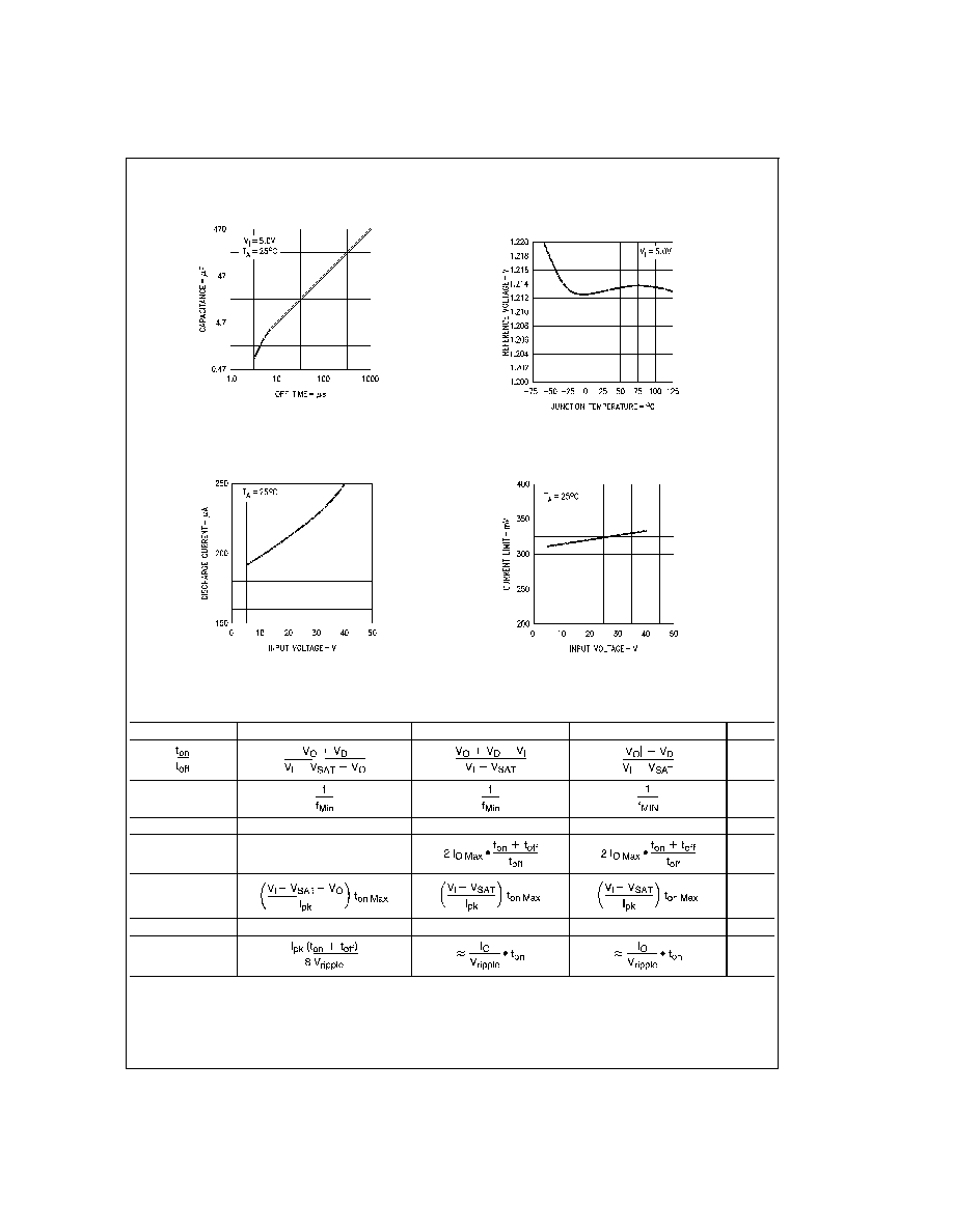
Typical Performance Characteristics
Design Formulas
Characteristic
Step-Down
Step-Up
Inverting
Units
(t
on
+ t
off
) Max
µs
C
T
4 x 10
-5
t
on
4 x 10
-5
t
on
4 x 10
-5
t
on
µF
I
pk
2 I
O Max
A
L
Min
µH
R
SC
0.33/I
pk
0.33/I
pk
0.33/I
pk
C
O
µF
Note 6: V
SAT
= Saturation voltage of the switching element.
V
D
= Forward voltage of the flyback diode.
C
T
vs OFF Time
DS010057-6
Reference Voltage vs
Junction Temperature
DS010057-7
Discharge Current vs
Input Voltage
DS010057-8
Current Limit Sense
Voltage vs Input Voltage
DS010057-9
5
www.national.com