DS78C120
Dual CMOS Compatible Differential Line Receiver
General Description
The DS78C120 is a high performance, dual differential,
CMOS compatible line receiver for both balanced and unbal-
anced digital data transmission. The inputs are compatible
with EIA, Federal and MIL standards.
Input specifications meet or exceed those of the popular
DS7820 line receiver.
The line receiver will discriminate a
±
200 mV input signal
over a common-mode range of
±
10V and a
±
300 mV signal
over a range of
±
15V.
Circuit features include hysteresis and response control for
applications where controlled rise and fall times and/or high
frequency noise rejection are desirable. Threshold offset
control is provided for fail-safe detection, should the input be
open or short. Each receiver includes a 180
terminating re-
sistor and the output gate contains a logic strobe for time dis-
crimination. The DS78C120 is specified over a -55∞C to
+125∞C temperature range.
Features
n
Full compatibility with EIA Standards RS232-C, RS422
and RS423, Federal Standards 1020, 1030 and
MIL-188-114
n
Input voltage range of
±
15V (differential or
common-mode)
n
Separate strobe input for each receiver
n
1/2 V
CC
strobe threshold for CMOS compatibility
n
5k typical input impedance
n
50 mV input hysteresis
n
200 mV input threshold
n
Operation voltage range = 4.5V to 15V
n
Separate fail-safe mode
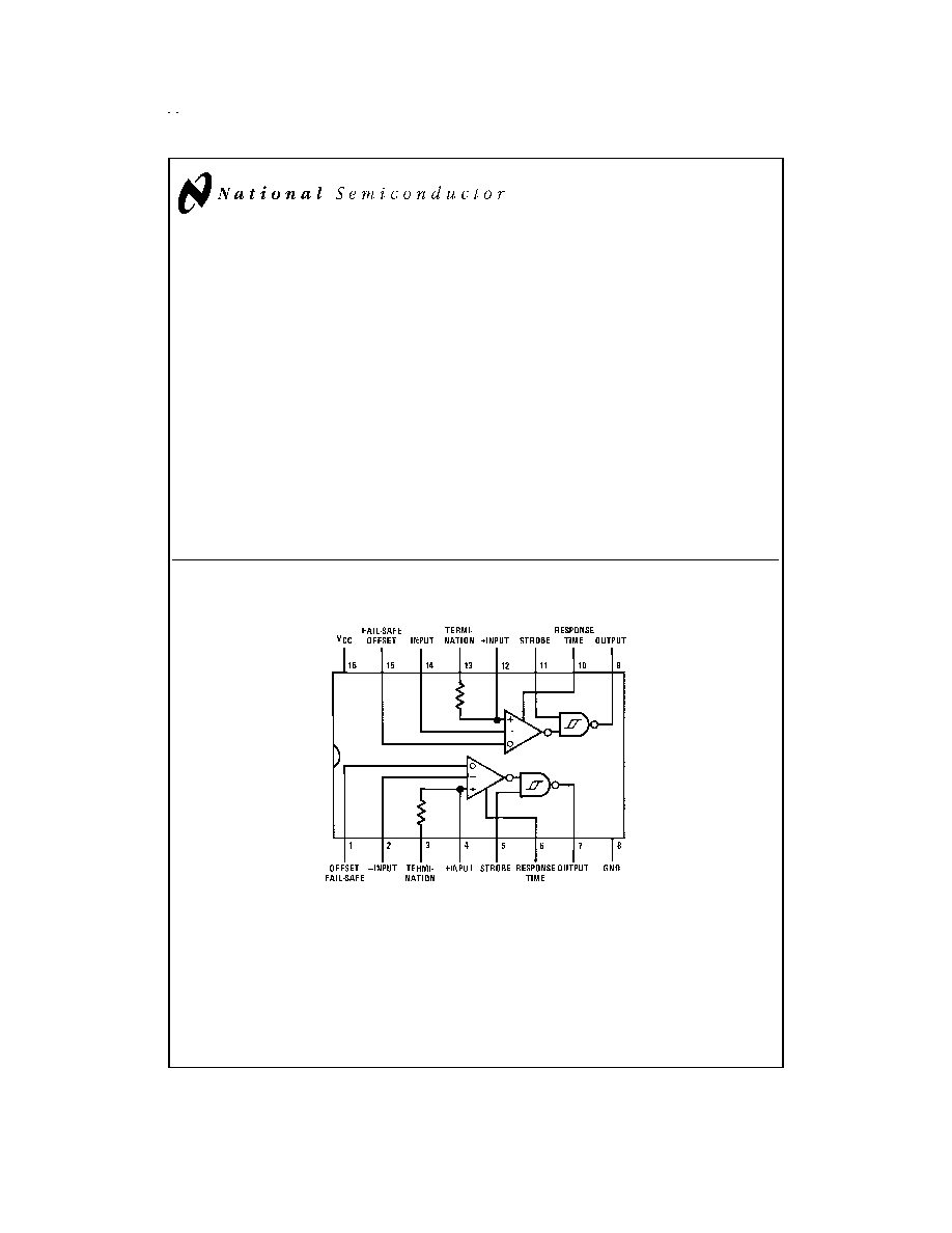
Connection Diagram
TRI-STATE
Æ
is a registered trademark of National Semiconductor Corporation.
Dual-In-Line Package
DS005801-1
Top View
For Complete Military Product Specifications,
refer to the appropriate SMD or MDS.
Order Number DS78C120J/883
See NS Package Number J16A
May 1999
DS78C120
Dual
CMOS
Compatible
Differential
Line
Receiver
© 1999 National Semiconductor Corporation
DS005801
www.national.com
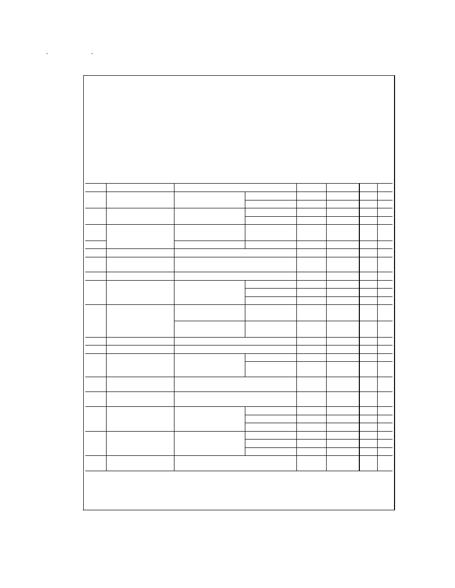
Absolute Maximum Ratings
(Note 2)
If Military/Aerospace specified devices are required,
please contact the National Semiconductor Sales Office/
Distributors for availability and specifications.
Supply Voltage
18V
Input Voltage
±
25V
Strobe Voltage
18V
Output Sink Current
50 mA
Maximum Power Dissipation (Note 1) at 25∞C
Cavity Package
1433 mW
Molded Package
1362 mW
Storage Temperature Range
-65∞C to +150∞C
Lead Temperature (Soldering, 4 seconds)
260∞C
Operating Conditions
Min
Max
Units
Supply Voltage (V
CC
)
4.5
15
V
Temperature (T
A
)
DS78C120
-55
+125
∞C
Common-Mode Voltage (V
CM
)
-15
+15
V
Note 1: Derate cavity package 9.6 mW/∞C; derate molded package
10.9 mW/∞C above 25∞C.
Electrical Characteristics
(Notes 3, 4)
Symbol
Parameter
Conditions
Min
Typ
Max Units
V
TH
Differential Threshold
I
OUT
= -200 µA,
-7V
V
CM
7V
0.06
0.2
V
Voltage
V
OUT
V
CC
- 1.2V
-15V
V
CM
15V
0.06
0.3
V
V
TL
Differential Threshold
I
OUT
= 1.6 mA,V
OUT
0.5V
-7V
V
CM
7V
-0.08
-0.2
V
Voltage
-15V
V
CM
15V
-0.08
-0.3
V
V
TH
Differential Threshold
I
OUT
= -200 µA,
-7V
V
CM
7V
0.47
0.7
V
Voltage Fail-Safe
V
OUT
V
CC
- 1.2V
V
TL
Offset = 5V
I
OUT
= 1.6 mA,V
OUT
0.5V
-7V
V
CM
7V
0.2
0.42
V
R
IN
Input Resistance
-15V
V
CM
15V, 0V
V
CC
15V
4
5
k
R
T
Line Termination
Resistance
T
A
= 25∞C
100
180
300
R
O
Offset Control Resistance
T
A
= 25∞C
56
k
I
IND
Data Input Current
0V
V
CC
15V
V
CM
= 10V
2
3.1
mA
(Unterminated)
V
CM
= 0V
0
-0.5
mA
V
CM
= -10V
-2
-3.1
mA
V
THB
Input Balance
I
OUT
= 200 µA, V
OUT
-7V
V
CM
7V
0.1
0.4
V
(Note 6)
V
CC
- 1.2V, R
S
= 500
I
OUT
= 1.6 mA,V
OUT
0.5V
-7V
V
CM
7V
-0.1
-0.4
V
R
S
= 500
V
OH
Logical "1" Output Voltage
I
OUT
= -200 µA, V
DIFF
= 1V
V
CC
- 1.2
V
CC
- 0.75
V
V
OL
Logical "0" Output Voltage
I
OUT
= 1.6 mA, V
DIFF
= -1V
0.25
0.5
V
I
CC
Power Supply Current
15V
V
CM
-15V,
V
CC
= 5.5V
8
15
mA
V
DIFF
= -0.5V
(Both Receivers)
V
CC
= 15V
15
30
mA
I
IN(1)
Logical "1" Strobe Input
Current
V
STROBE
= 15V, V
DIFF
= 3V
15
100
µA
I
IN(0)
Logical "0" Strobe Input
Current
V
STROBE
= 0V, V
DIFF
= -3V
-0.5
-100
µA
V
IH
Logical "1" Strobe Input
V
OL
0.5V, I
OUT
= 1.6 mA
V
CC
= 5V
3.5
2.5
V
Voltage
V
CC
= 10V
8.0
5.0
V
V
CC
= 15V
12.5
7.5
V
V
IL
Logical "0" Strobe Input
Voltage
V
OH
V
CC
- 1.2V,
V
CC
= 5V
2.5
1.5
V
I
OUT
= -200 µA
V
CC
= 10V
5.0
2.0
V
V
CC
= 15V
7.5
2.5
V
I
OS
Output Short-Circuit
Current
V
OUT
= 0V, V
CC
= 15V, V
STROBE
= 0V, (Note 5)
-5
-20
-40
mA
Note 2: "Absolute Maximum Ratings" are those values beyond which the safety of the device cannot be guaranteed. Except for "Operating Temperature Range" they
are not meant to imply that the devices should be operated at these limits. The table of "Electrical Characteristics" provides conditions for actual device operation.
Note 3: Unless otherwise specified min/max limits apply across the -55∞C to +125∞C temperature range for the DS78C120. All typical values for T
A
= 25∞C, V
CC
=
5V and V
CM
= 0V.
www.national.com
2
Electrical Characteristics
(Notes 3, 4) (Continued)
Note 4: All currents into device pins shown as positive, out of device pins as negative, all voltages referenced to ground unless otherwise noted. All values shown
as max or min on absolute value basis.
Note 5: Only one output at a time should be shorted.
Note 6: Refer to EIA-RS422 for exact conditions.
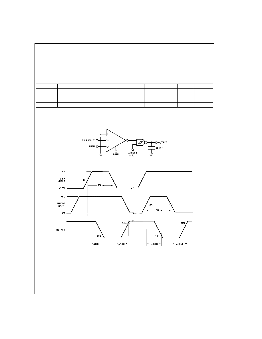
Switching Characteristics
V
CC
= 5V, T
A
= 25∞C
Symbol
Parameter
Conditions
Min
Typ
Max
Units
t
pd0(D)
Differential Input to "0" Output
C
L
= 50 pF
60
100
ns
t
pd1(D)
Differential Input to "1" Output
C
L
= 50 pF
100
150
ns
t
pd0(S)
Strobe Input to "0" Output
C
L
= 50 pF
30
70
ns
t
pd1(S)
Strobe Input to "1" Output
C
L
= 50 pF
100
150
ns
AC Test Circuit and Switching Time Waveforms
Differential and Strobe Input Signal
DS005801-3
*Includes probe and test fixture capacitance
DS005801-4
t
r
= t
f
10 ns
PRR = 1 MHz
Note: Optimum switching response is obtained by minimizing stray capacitance on Response Control pin (no external connection).
www.national.com
3
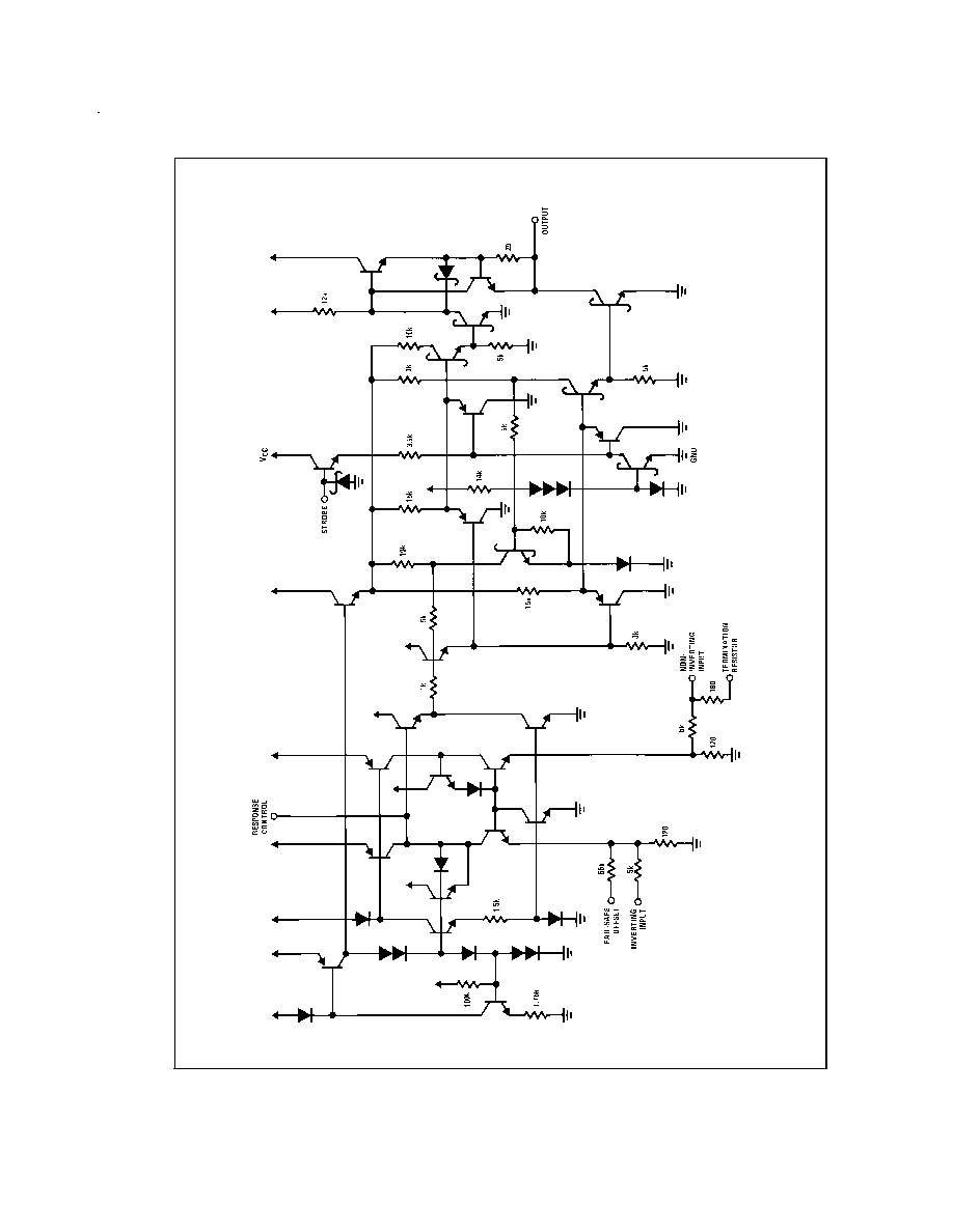
Schematic Diagram
(
1
/
2
Circuit Shown)
DS005801-2
www.national.com
4

Application Hints
The DS78C120 may be used a level transistor to interface between
±
12V MOS, ECL, TTL and CMOS. To configure, bias either
input to voltage equal to
1
/
2
the voltage of the input signal, and the other input to the driving gate.
Balanced Data Transmission
DS005801-5
Unbalanced Data Transmission
DS005801-6
Logic Level Translator
DS005801-7
DS005801-8
www.national.com
5