
54AC257
∑
54ACT257
Quad 2-Input Multiplexer with TRI-STATE
Æ
Outputs
General Description
The 'AC/'ACT257 is a quad 2-input multiplexer with
TRI-STATE outputs. Four bits of data from two sources can
be selected using a Common Data Select input. The four
outputs present the selected data in true (noninverted) form.
The outputs may be switched to a high impedance state by
placing a logic HIGH on the common Output Enable (OE) in-
put,
allowing
the
outputs
to
interface
directly
with
bus-oriented systems.
Features
n
I
CC
and I
OZ
reduced by 50%
n
Multiplexer expansion by tying outputs together
n
Noninverting TRI-STATE outputs
n
Outputs source/sink 24 mA
n
'ACT257 has TTL-compatible inputs
n
Standard Military Drawing (SMD)
-- 'AC257: 5962-88703
-- 'ACT257: 5962-89689
Logic Symbols
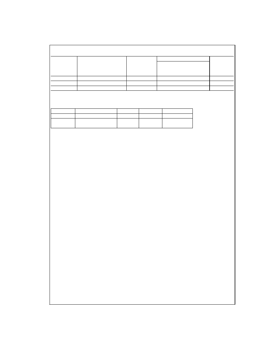
Pin Names
Description
S
Common Data Select Input
OE
TRI-STATE Output Enable Input
I
0a
≠I
0d
Data Inputs from Source 0
I
1a
≠I
1d
Data Inputs from Source 1
Z
a
≠Z
d
TRI-STATE Multiplexer Outputs
TRI-STATE
Æ
is a registered trademark of National Semiconductor Corporation.
FACT
TM
is a trademark of Fairchild Semiconductor Corporation.
DS100286-1
IEEE/IEC
DS100286-2
July 1998
54AC257
∑
54ACT257
Quad
2-Input
Multiplexer
with
TRI-ST
A
T
E
Outputs
© 1998 National Semiconductor Corporation
DS100286
www.national.com
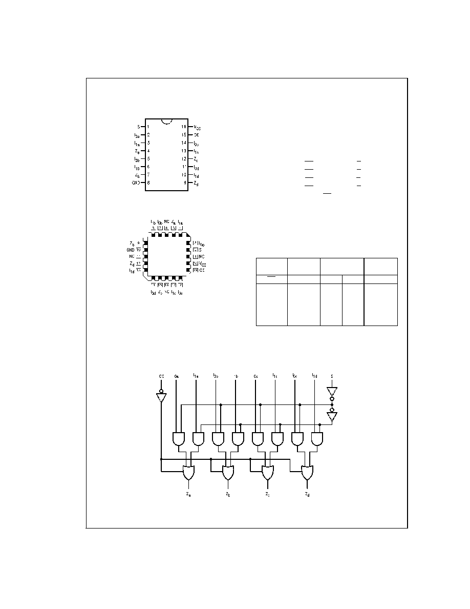
Connection Diagrams
Functional Description
The
'AC/'ACT257
is
quad
2-input
multiplexer
with
TRI-STATE outputs. It selects four bits of data from two
sources under control of a Common Data Select input. When
the Select input is LOW, the I
0x
inputs are selected and when
Select is HIGH, the I
1x
inputs are selected. The data on the
selected inputs appears at the outputs in true (noninverted)
form. The device is the logic implementation of a 4-pole,
2-position switch where the position of the switch is deter-
mined by the logic levels supplied to the Select input. The
logic equations for the outputs are shown below:
Z
a
= OE ∑ (1
1a
∑ S + I
0a
∑ S)
Z
b
= OE ∑ (1
1b
∑ S + I
0b
∑ S)
Z
c
= OE ∑ (1
1c
∑ S + I
0c
∑ S)
Z
d
= OE ∑ (1
1d
∑ S + I
0d
∑ S)
When the Output Enable (OE) is HIGH, the outputs are
forced to a high impedance state. If the outputs are tied to-
gether, all but one device must be in the high impedance
state to avoid high currents that would exceed the maximum
ratings. Designers should ensure the Output Enable signals
to TRI-STATE devices whose outputs are tied together are
designed so there is no overlap.
Truth Table
Output
Select
Data
Outputs
Enable
Input
Inputs
OE
S
I
0
I
1
Z
H
X
X
X
Z
L
H
X
L
L
L
H
X
H
H
L
L
L
X
L
L
L
H
X
H
H = HIGH Voltage Level
L = LOW Voltage Level
X = Immaterial
Z = High Impedance
Logic Diagram
Pin Assignment for
DIP and Flatpak
DS100286-3
Pin Assignment for LCC
DS100286-4
DS100286-5
Please note that this diagram is provided only for the understanding of logic operations and should not be used to estimate propagation delays.
www.national.com
2
Absolute Maximum Ratings
(Note 1)
If Military/Aerospace specified devices are required,
please contact the National Semiconductor Sales Office/
Distributors for availability and specifications.
Supply Voltage (V
CC
)
-0.5V to +7.0V
DC Input Diode Current (I
IK
)
V
I
= -0.5V
-20 mA
V
I
= V
CC
+0.5V
+20 mA
DC Input Voltage (V
I
)
-0.5V to V
CC
+0.5V
DC Output Diode Current (I
OK
)
V
O
= -0.5V
-20 mA
V
O
= V
CC
+0.5V
+20 mA
DC Output Voltage (V
O
)
-0.5V to V
CC
+0.5V
DC Output Source or Sink Current
(I
O
)
±
50 mA
DC V
CC
or Ground Current
Per Output Pin (I
CC
or I
GND
)
±
50 mA
Storage Temperature (T
STG
)
-65∞C to +150∞C
Junction Temperature (T
J
)
CDIP
175∞C
Recommended Operating
Conditions
Supply Voltage (V
CC
)
'AC
2.0V to 6.0V
'ACT
4.5V to 5.5V
Input Voltage (V
I
)
0V to V
CC
Output Voltage (V
O
)
0V to V
CC
Operating Temperature (T
A
)
54AC/ACT
-55∞C to +125∞C
Minimum Input Edge Rate (
V/
t)
'AC Devices
V
IN
from 30% to 70% of V
CC
V
CC
@
3.3V, 4.5V, 5.5V
125 mV/ns
Minimum Input Edge Rate (
V/
t)
'ACT Devices
V
IN
from 0.8V to 2.0V
V
CC
@
4.5V, 5.5V
125 mV/ns
Note 1: Absolute maximum ratings are those values beyond which damage
to the device may occur. The databook specifications should be met, without
exception, to ensure that the system design is reliable over its power supply,
temperature, and output/input loading variables. National does not recom-
mend operation of FACT
TM
circuits outside databook specifications.
DC Characteristics for 'AC Family Devices
54AC
Symbol
Parameter
V
CC
T
A
=
Units
Conditions
(V)
-55∞C to +125∞C
Guaranteed
Limits
V
IH
Minimum High
3.0
2.1
V
OUT
= 0.1V
Level Input
4.5
3.15
V
or V
CC
- 0.1V
Voltage
5.5
3.85
V
IL
Maximum Low
3.0
0.9
V
OUT
= 0.1V
Level Input
4.5
1.35
V
or V
CC
- 0.1V
Voltage
5.5
1.65
V
OH
Minimum High
3.0
2.9
I
OUT
= -50 µA
Level Output
4.5
4.4
V
Voltage
5.5
5.4
(Note 2)
V
IN
= V
IL
or V
IH
3.0
2.4
-12 mA
4.5
3.7
V
I
OH
-24 mA
5.5
4.7
-24 mA
V
OL
Maximum Low
3.0
0.1
I
OUT
= 50 µA
Level Output
4.5
0.1
V
Voltage
5.5
0.1
(Note 2)
V
IN
= V
IL
or V
IH
3.0
0.50
12 mA
4.5
0.50
V
I
OL
24 mA
5.5
0.50
24 mA
I
IN
Maximum Input
5.5
±
1.0
µA
V
I
= V
CC
, GND
Leakage Current
3
www.national.com
DC Characteristics for 'AC Family Devices
(Continued)
54AC
Symbol
Parameter
V
CC
T
A
=
Units
Conditions
(V)
-55∞C to +125∞C
Guaranteed
Limits
I
OZ
Maximum
V
I
(OE) = V
IL
, V
IH
TRI-STATE
5.5
±
10.0
µA
V
I
= V
CC
, GND
Leakage Current
V
O
= V
CC
, GND
I
OLD
(Note 3) Minimum
Dynamic Output
Current
5.5
50
mA
V
OLD
= 1.65V Max
I
OHD
5.5
-50
mA
V
OHD
= 3.85V Min
I
CC
Maximum Quiescent
5.5
80.0
µA
V
IN
= V
CC
Supply Current
or GND
Note 2: All outputs loaded; thresholds on input associated with output under test.
Note 3: Maximum test duration 2.0 ms, one output loaded at a time.
Note 4: I
IN
and I
CC
@
3.0V are guaranteed to be less than or equal to the respective limit
@
5.5V V
CC
.
Note 5: I
CC
for 54AC
@
25∞C is identical to 74AC
@
25∞C.
DC Characteristics for 'ACT Family Devices
54ACT
Symbol
Parameter
V
CC
T
A
=
Units
Conditions
(V)
-55∞C to +125∞C
Guaranteed
Limits
V
IH
Minimum High
Level Input
Voltage
4.5
2.0
V
V
OUT
= 0.1V
5.5
2.0
or V
CC
- 0.1V
V
IL
Maximum Low
Level Input
Voltage
4.5
0.8
V
V
OUT
= 0.1V
5.5
0.8
or V
CC
- 0.1V
V
OH
Minimum High
Level Output
Voltage
4.5
4.4
V
I
OUT
= -50 µA
5.5
5.4
(Note 6)
V
IN
= V
IL
or V
IH
4.5
3.70
V
I
OH
-24 mA
5.5
4.70
-24 mA
V
OL
Maximum Low
Level Output
Voltage
4.5
0.1
V
I
OUT
= 50 µA
5.5
0.1
(Note 6)
V
IN
= V
IL
or V
IH
4.5
0.50
V
I
OL
24 mA
5.5
0.50
24 mA
I
IN
Maximum Input
5.5
±
1.0
µA
V
I
= V
CC
, GND
Leakage Current
I
OZ
Maximum TRI-STATE
5.5
±
10.0
µA
V
I
= V
IL
, V
IH
Leakage Current
V
O
= V
CC
, GND
I
CCT
Maximum
5.5
1.6
mA
V
I
= V
CC
- 2.1V
I
CC
/Input
I
OLD
(Note 7) Minimum
Dynamic Output
Current
5.5
50
mA
V
OLD
= 1.65V Max
I
OHD
5.5
-50
mA
V
OHD
= 3.85V Min
www.national.com
4
DC Characteristics for 'ACT Family Devices
(Continued)
54ACT
Symbol
Parameter
V
CC
T
A
=
Units
Conditions
(V)
-55∞C to +125∞C
Guaranteed
Limits
I
CC
Maximum Quiescent
5.5
80.0
µA
V
IN
= V
CC
Supply Current
or GND
Note 6: All outputs loaded; thresholds on input associated with output under test.
Note 7: Maximum test duration 2.0 ms, one output loaded at a time.
Note 8: I
CC
for 54ACT
@
25∞C is identical to 74ACT
@
25∞C.
AC Electrical Characteristics
54AC
Symbol
Parameter
V
CC
T
A
= -55∞C
Units
(V)
to +125∞C
(Note 9)
C
L
= 50 pF
t
PLH
Propagation Delay
3.3
1.0
11.0
ns
I
n
to Z
n
5.0
1.0
8.0
t
PHL
Propagation Delay
3.3
1.0
11.0
ns
I
n
to Z
n
5.0
1.0
8.5
t
PLH
Propagation Delay
3.3
1.0
14.5
ns
S to Z
n
5.0
1.0
11.0
t
PHL
Propagation Delay
3.3
1.0
14.5
ns
S to Z
n
5.0
1.0
11.0
t
PZH
Output Enable Time
3.3
1.0
13.0
ns
5.0
1.0
10.0
t
PZL
Output Enable Time
3.3
1.0
11.0
ns
5.0
1.0
9.5
t
PHZ
Output Disable Time
3.3
1.0
13.0
ns
5.0
1.0
11.0
t
PLZ
Output Disable Time
3.3
1.0
10.5
ns
5.0
1.0
9.5
Note 9: Voltage Range 3.3 is 3.0V
±
0.3V
Voltage Range 5.0 is 5.0V
±
0.5V
AC Electrical Characteristics
54ACT
Symbol
Parameter
V
CC
T
A
= -55∞C
Units
(V)
to +125∞C
(Note 10)
C
L
= 50 pF
t
PLH
Propagation Delay
5.0
1.0
8.0
ns
I
n
to Z
n
t
PHL
Propagation Delay
5.0
1.0
9.5
ns
I
n
to Z
n
t
PLH
Propagation Delay
5.0
1.0
11.0
ns
S to Z
n
t
PHL
Propagation Delay
5.0
1.0
11.5
ns
S to Z
n
t
PZH
Output Enable Time
5.0
1.0
9.5
ns
5
www.national.com
AC Electrical Characteristics
(Continued)
54ACT
Symbol
Parameter
V
CC
T
A
= -55∞C
Units
(V)
to +125∞C
(Note 10)
C
L
= 50 pF
t
PZL
Output Enable Time
5.0
1.0
9.5
ns
t
PHZ
Output Disable Time
5.0
1.0
10.5
ns
t
PLZ
Output Disable Time
5.0
1.0
9.5
ns
Note 10: Voltage Range 5.0 is 5.0V
±
0.5V
Capacitance
Symbol
Parameter
Typ
Units
Conditions
C
IN
Input Capacitance
4.5
pF
V
CC
= OPEN
C
PD
Power Dissipation
50.0
pF
V
CC
= 5.0V
Capacitance
www.national.com
6

Physical Dimensions
inches (millimeters) unless otherwise noted
20 Terminal Ceramic Leadless Chip Carrier (L)
NS Package Number E20A
16 Lead Ceramic Flatpak (F)
NS Package Number W16A
7
www.national.com
LIFE SUPPORT POLICY
NATIONAL'S PRODUCTS ARE NOT AUTHORIZED FOR USE AS CRITICAL COMPONENTS IN LIFE SUPPORT DE-
VICES OR SYSTEMS WITHOUT THE EXPRESS WRITTEN APPROVAL OF THE PRESIDENT OF NATIONAL SEMI-
CONDUCTOR CORPORATION. As used herein:
1. Life support devices or systems are devices or sys-
tems which, (a) are intended for surgical implant into
the body, or (b) support or sustain life, and whose fail-
ure to perform when properly used in accordance
with instructions for use provided in the labeling, can
be reasonably expected to result in a significant injury
to the user.
2. A critical component in any component of a life support
device or system whose failure to perform can be rea-
sonably expected to cause the failure of the life support
device or system, or to affect its safety or effectiveness.
National Semiconductor
Corporation
Americas
Tel: 1-800-272-9959
Fax: 1-800-737-7018
Email: support@nsc.com
www.national.com
National Semiconductor
Europe
Fax: +49 (0) 1 80-530 85 86
Email: europe.support@nsc.com
Deutsch Tel: +49 (0) 1 80-530 85 85
English
Tel: +49 (0) 1 80-532 78 32
FranÁais Tel: +49 (0) 1 80-532 93 58
Italiano
Tel: +49 (0) 1 80-534 16 80
National Semiconductor
Asia Pacific Customer
Response Group
Tel: 65-2544466
Fax: 65-2504466
Email: sea.support@nsc.com
National Semiconductor
Japan Ltd.
Tel: 81-3-5620-6175
Fax: 81-3-5620-6179
54AC257
∑
54ACT257
Quad
2-Input
Multiplexer
with
TRI-ST
A
T
E
Outputs
National does not assume any responsibility for use of any circuitry described, no circuit patent licenses are implied and National reserves the right at any time without notice to change said circuitry and specifications.