CLC401
Fast Settling, Wideband High Gain Monolithic Op Amp
General Description
The CLC401 is a wideband, fast settling op amp designed
for applications requiring gains greater than
±
7. Constructed
using an advanced complementary bipolar process and a
proprietary design, the CLC401 features dynamic perfor-
mance far beyond that of typical high speed monolithic op
amps. For example, at a gain of +20, the -3dB bandwidth is
150MHz and the rise/fall time is only 2.5ns.
The wide bandwidth and linear phase (0.2∞ deviation from
linear at 50MHz) and a very flat gain response makes the
CLC401 ideal for many digital communication system appli-
cations. For example, demodulators need both DC coupling
and high frequency amplification-requirements that are ordi-
narily difficult to meet.
The very fast 10ns settling to 0.1% and the ability to drive
capacitive loads lend themselves well to flash A/D applica-
tions. Systems employing D/A converters also benefit from
the settling time and also by the fact that current-to-voltage
transimpedance amplification is easily accomplished.
The CLC401 provides a quick, effective design solution. Its
stable operation over the entire
±
7 to
±
50 gain range pre-
cludes the need for external compensation. And, unlike
many other high speed-op amps, the CLC401's power dis-
sipation of 150mW is compatible with designs which must
limit total power dissipation or power supply requirements.
The CLC401 is based on National's proprietary op amp
topology that uses current feedback instead of the usual
voltage feedback. This unique design has many advantages
over conventional designs (such as settling time that is
relatively independent of gain), yet it is used in basically the
same way (see the gain equations in
Figure 1 and Figure 2).
However, an understanding of the topology will aid in achiev-
ing the best performance. The discussion below will proceed
for the non-inverting gain configuration with the inverting
mode analysis being very similar.
Enhanced Solutions (Military/Aerospace)
SMD Number: 5962-89973
Space level versions also available.
For more information, visit http://www.national.com/mil
Features
n
-3dB bandwidth of 150MHz
n
0.1% settling in 10ns
n
Low power, 150mW
n
Overload and short circuit protected
n
Stable without compensation
n
Recommended gain range,
±
7 to
±
50
Applications
n
Flash, precision A/D conversion
n
Photodiode, CCD preamps
n
IF processors
n
High speed modems, radios
n
Line drivers
n
DC coupled log amplifiers
n
High speed communications
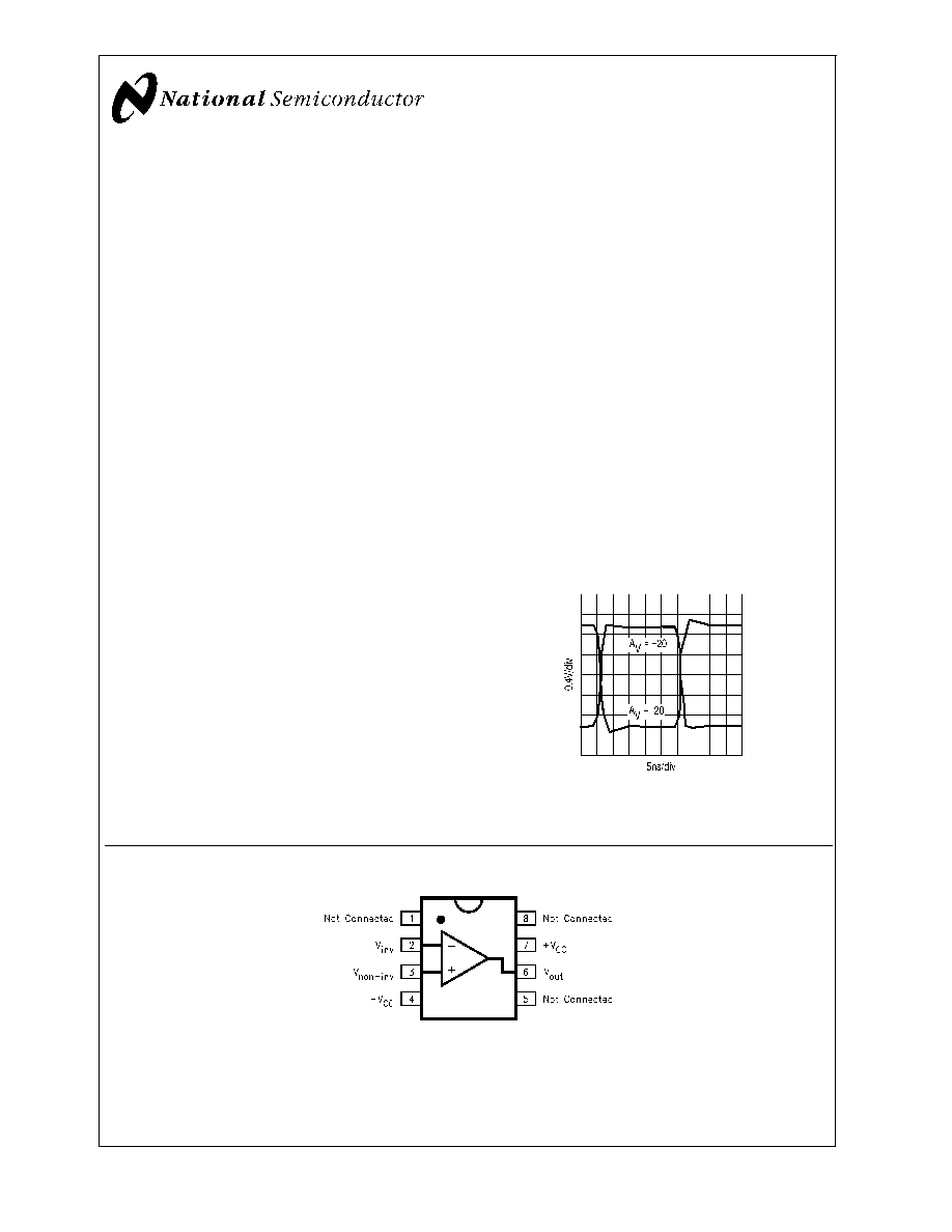
Pulse Response
01274418
Connection Diagram
01274417
Pinout
DIP & SOIC
June 2001
CLC401
Fast
Settling,
W
ideband
High
Gain
Monolithic
Op
Amp
© 2001 National Semiconductor Corporation
DS012744
www.national.com
Absolute Maximum Ratings
(Note 1)
If Military/Aerospace specified devices are required,
please contact the National Semiconductor Sales Office/
Distributors for availability and specifications.
Supply Voltage (V
CC
)
±
7V
I
OUT
Output is short circuit protected to
ground, but maximum reliability will
be maintained if I
OUT
does not
exceed...
60mA
Common Mode Input Voltage
±
V
CC
Differential Input Voltage
5V
Junction Temperature Range
+150∞C
Operating Temperature Range
-40∞C to +85∞C
Storage Temperature Range
-65∞C to +150∞C
Lead Solder Duration (+300∞C)
10 sec
Operating Ratings
Thermal Resistance
Package
(
JC
)
(
JA
)
MDIP
70∞C/W
125∞C/W
SOIC
65∞C/W
145∞C/W
Electrical Characteristics
(A
V
= +20, V
CC
=
±
5V, R
L
= 100
, R
f
=1.5k
; unless specified).
Symbol
Parameter
Conditions
Typ
Max/Min Ratings
(Note 2)
Units
Ambient Temperature
CLC401AJ
+25∞C
-40∞C
+25∞C
+85∞C
Frequency Domain Response
SSBW
-3dB Bandwidth
V
OUT
<
2V
PP
150
>
100
>
100
>
70
MHz
LSBW
V
OUTt
<
5V
PP
100
>
65
>
65
>
55
MHz
Gain Flatness
V
OUT
<
2V
PP
GFPL
Peaking
<
25MHz
0
<
0.1
<
0.1
<
0.1
dB
GFPH
Peaking
>
25MHz
0
<
0.2
<
0.2
<
0.2
dB
GFR
Rolloff
<
50MHz
0.2
<
1.0
<
1.0
<
1.3
dB
LPD
Linear Phase Deviation
DC to 50MHz
0.2
<
1.0
<
1.0
<
1.5
deg
Time Domain Response
TRS
Rise and Fall Time
2V Step
2.5
<
3.5
<
3.5
<
5.0
ns
TRL
5V Step
5
<
7.0
<
7.0
<
8.0
ns
TS
Settling Time to
±
0.1%
2V Step
10
<
15
<
15
<
15
ns
OS
Overshoot
2V Step
0
<
10
<
10
<
10
%
SR
Slew Rate
1200
>
800
>
800
>
700
V/µs
Distortion And Noise Response
HD2
2nd Harmonic Distortion
2V
PP
, 20MHz
-45
<
-35
<
-35
<
-35
dBc
HD3
3rd Harmonic Distortion
2V
PP
, 20MHz
-60
<
-50
<
-50
<
-45
dBc
Equivalent Input Noise
SNF
Noise Floor
>
1MHz
-158
<
-155
<
-155
<
-154
dBm
(1Hz)
INV
Integrated Noise
1MHz to 150MHz
35
<
50
<
50
<
55
µV
Static, DC Performance
VIO
Input Offset Voltage (Note 3)
3
±
10.0
±
6.0
±
11.0
mV
DVIO
Average Temperature Coefficient
20
±
50
≠
±
50
µV/∞C
IBN
Input Bias Current (Note 3)
Non-Inverting
10
±
36
±
20
±
20
µA
DIBN
Average Temperature Coefficient
100
±
200
≠
±
100
nA/∞C
IBI
Input Bias Current (Note 3)
Inverting
10
46
30
40
µA
DIBI
Average Temperature Coefficient
100
±
200
≠
±
100
nA/∞C
PSRR
Power Supply Rejection Ratio
55
50
50
50
dB
CMRR
Common Mode Rejection Ratio
55
50
50
50
dB
ICC
Supply Current (Note 3)
No Load
15
21
21
21
mA
Miscellaneous Performance
RIN
Non-Inverting Input
Resistance
200
>
50
>
100
>
100
k
CIN
Capacitance
0.5
<
2.5
<
2.5
<
2.5
pF
CLC401
www.national.com
3
Electrical Characteristics
(Continued)
(A
V
= +20, V
CC
=
±
5V, R
L
= 100
, R
f
=1.5k
; unless specified).
Symbol
Parameter
Conditions
Typ
Max/Min Ratings
(Note 2)
Units
RO
Output Impedance
at DC
0.2
<
0.3
<
0.3
<
0.3
VO
Output Voltage Range
No Load
3.5
>
3.0
>
3.2
>
3.2
V
CMIR
Common Mode Input Range
For Rated Performance
2.8
>
2.0
>
2.5
>
2.5
V
IO
Output Current
60
>
35
>
50
>
50
mA
Note 1: "Absolute Maximum Ratings" are those values beyond which the safety of the device cannot be guaranteed. They are not meant to imply that the devices
should be operated at these limits. The table of "Electrical Characteristics" specifies conditions of device operation.
Note 2: Max/min ratings are based on product characterization and simulation. Individual parameters are tested as noted. Outgoing quality levels are determined
from tested parameters.
Note 3: AJ-level: spec. is 100% tested at +25∞C.
CLC401
www.national.com
4

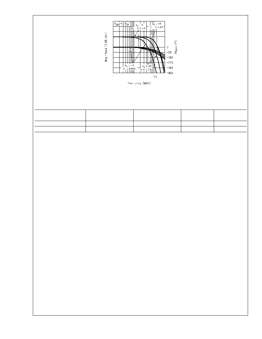
Typical Performance Characteristics
(T
A
= 25∞, A
V
= +20, V
CC
=
±
5V, R
L
= 100
: Unless Speci-
fied).
Non-Inverting Frequency Response
Inverting Frequency Response
01274401
01274402
Frequency Response for Various R
L
s
Open-Loop Transimpedance Gain, Z(s)
01274403
01274404
2nd and 3rd Harmonic Distortion
2-Tone,3rd Order, Intermodulation Intercept
01274405
01274406
CLC401
www.national.com
5