TL F 10189
DM54LS502DM74LS502
8-Bit
Successive
Approximation
Register
April 1992
DM54LS502 DM74LS502
8-Bit Successive Approximation Register
General Description
The LS502 is an 8-bit register with the interstage logic nec-
essary to perform serial-to-parallel conversion and provide
an active LOW Conversion Complete (CC) signal coincident
with storage of the eighth bit An active LOW Start (S) input
performs synchronous initialization which forces Q7 LOW
and all other outputs HIGH Subsequent clocks shift this Q7
LOW signal downstream which simultaneously backfills the
register such that the first serial data (D input) bit is stored in
Q7 the second bit in Q6 the third in Q5 etc The serial
input data is also synchronized by an auxiliary flip-flop and
brought out on Q
D
Designed primarily for use in the successive approximation
technique for analog-to-digital conversion the LS502 can
also be used as a serial-to-parallel converter ring counter
and as the storage and control element in recursive digital
routines
Features
Y
Low power Schottky version of 2502
Y
Storage and control for successive approximation A to
D conversion
Y
Performs serial-to-parallel conversion
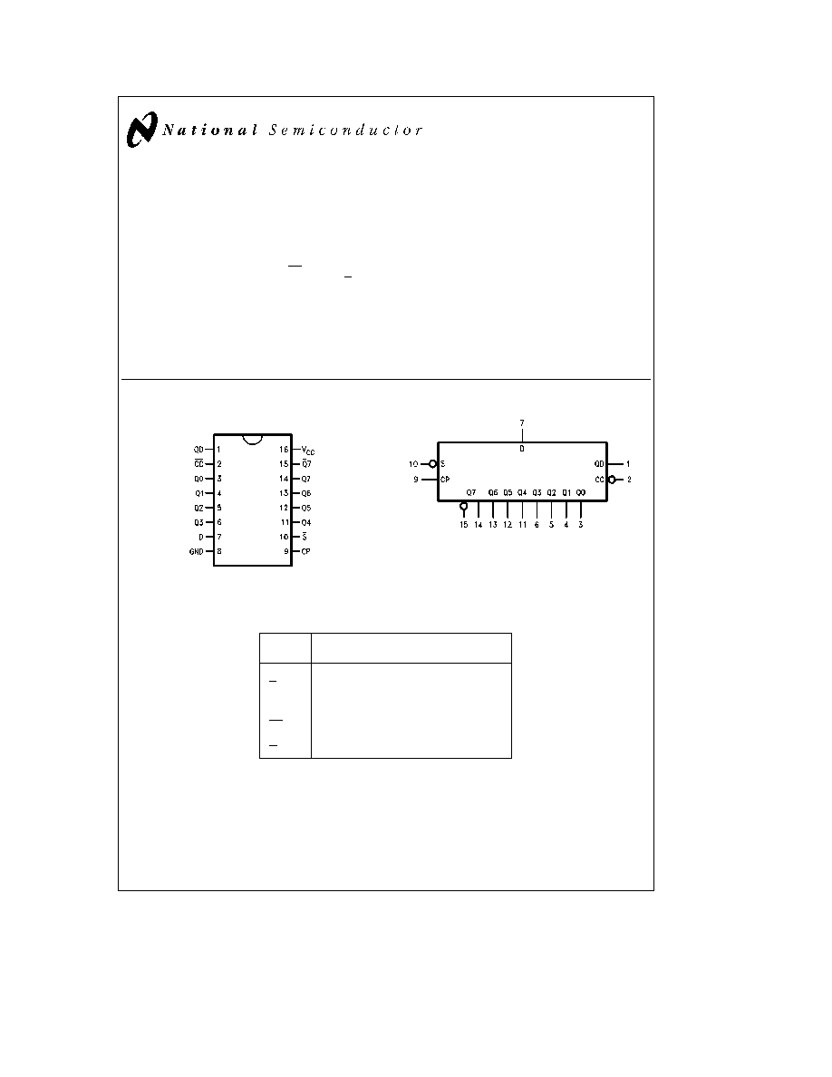
Connection Diagram
Dual-In-Line Package
TL F 10189 ≠ 1
Order Number DM54LS502J DM54LS502W
DM74LS502WM or DM74LS502N
See NS Package Number J16A M16B N16E or W16A
Logic Symbol
TL F 10189 ≠ 2
V
CC
e
Pin 16
GND
e
Pin 8
Pin
Description
Names
D
Serial Data Input
S
Start Input (Active LOW)
CP
Clock Pulse Input (Active Rising Edge)
Q
D
Synchronized Serial Data Output
CC
Conversion Complete Output (Active LOW)
Q0 ≠ Q7
Parallel Register Outputs
Q7
Complement of Q7 Output
C1995 National Semiconductor Corporation
RRD-B30M105 Printed in U S A
Absolute Maximum Ratings
(Note)
If Military Aerospace specified devices are required
please contact the National Semiconductor Sales
Office Distributors for availability and specifications
Supply Voltage
7V
Input Voltage
7V
Operating Free Air Temperature Range
DM54LS
b
55 C to
a
125 C
DM74LS
0 C to
a
70 C
Storage Temperature Range
b
65 C to
a
150 C
Note
The ``Absolute Maximum Ratings'' are those values
beyond which the safety of the device cannot be guaran-
teed The device should not be operated at these limits The
parametric values defined in the ``Electrical Characteristics''
table are not guaranteed at the absolute maximum ratings
The ``Recommended Operating Conditions'' table will define
the conditions for actual device operation
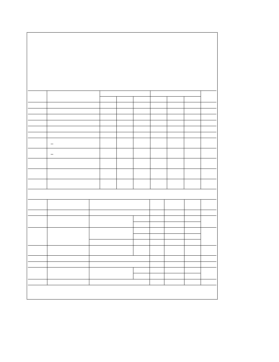
Recommended Operating Conditions
Symbol
Parameter
DM54LS502
DM74LS502
Units
Min
Nom
Max
Min
Nom
Max
V
CC
Supply Voltage
4 5
5
5 5
4 75
5
5 25
V
V
IH
High Level Input Voltage
2
2
V
V
IL
Low Level Input Voltage
0 7
0 8
V
I
OH
High Level Output Current
b
0 4
b
0 4
mA
I
OL
Low Level Output Current
4
8
mA
T
A
Free Air Operating Temperature
b
55
125
0
70
C
t
s
(H)
Setup Time HIGH or LOW
5
16
ns
t
s
(L)
S to CP
5
16
t
h
(H)
Hold Time HIGH or LOW
5
0
ns
t
h
(L)
S to CP
5
0
t
s
(H)
Setup Time HIGH or LOW
5
8
ns
t
s
(L)
D to CP
5
8
t
h
(H)
Hold Time HIGH or LOW
5
10
ns
t
h
(L)
D to CP
5
10
t
w
(H)
CP Pulse Width HIGH or LOW
20
46
ns
t
w
(L)
20
46
Electrical Characteristics
over recommended operating free air temperature range (unless otherwise noted)
Symbol
Parameter
Conditions
Min
Typ
Max
Units
(Note 1)
V
I
Input Clamp Voltage
V
CC
e
Min I
I
e b
18 mA
b
1 5
V
V
OH
High Level Output
V
CC
e
Min I
OH
e
Max
DM54
2 5
V
Voltage
V
IL
e
Max
DM74
2 7
V
OL
Low Level Output
V
CC
Min I
OL
e
Max
DM54
0 4
Voltage
V
IH
e
Min
DM74
0 5
V
I
OL
e
4 mA V
CC
e
Min
DM74
0 4
I
I
Input Current
Max
V
CC
e
Max V
I
e
7V
DM74
0 1
mA
Input Voltage
V
I
e
10V
DM54
I
IH
High Level Input Current
V
CC
e
Max V
I
e
2 7V
20
m
A
I
IL
Low Level Input Current
V
CC
e
Max V
I
e
0 4V
b
0 8
mA
I
OS
Short Circuit
V
CC
e
Max
DM54
b
20
b
100
mA
Output Current
(Note 2)
DM74
b
20
b
100
I
CC
Supply Current
V
CC
e
Max
65
mA
Note 1
All typicals are at V
CC
e
5V T
A
e
25 C
Note 2
Note more than one output should be shorted at a time and the duration should not exceed one second
2
Switching Characteristics
V
CC
e a
5 0V T
A
e a
25 C
Symbol
Parameter
DM54LS502
DM74LS502
Units
R
L
e
2 kX C
L
e
15 pF
Min
Max
Min
Max
f
max
Maximum Clock Frequency
25
15
MHz
t
PLH
Propagation Delay
35
35
ns
t
PHL
CP to Q
n
or CC
25
25
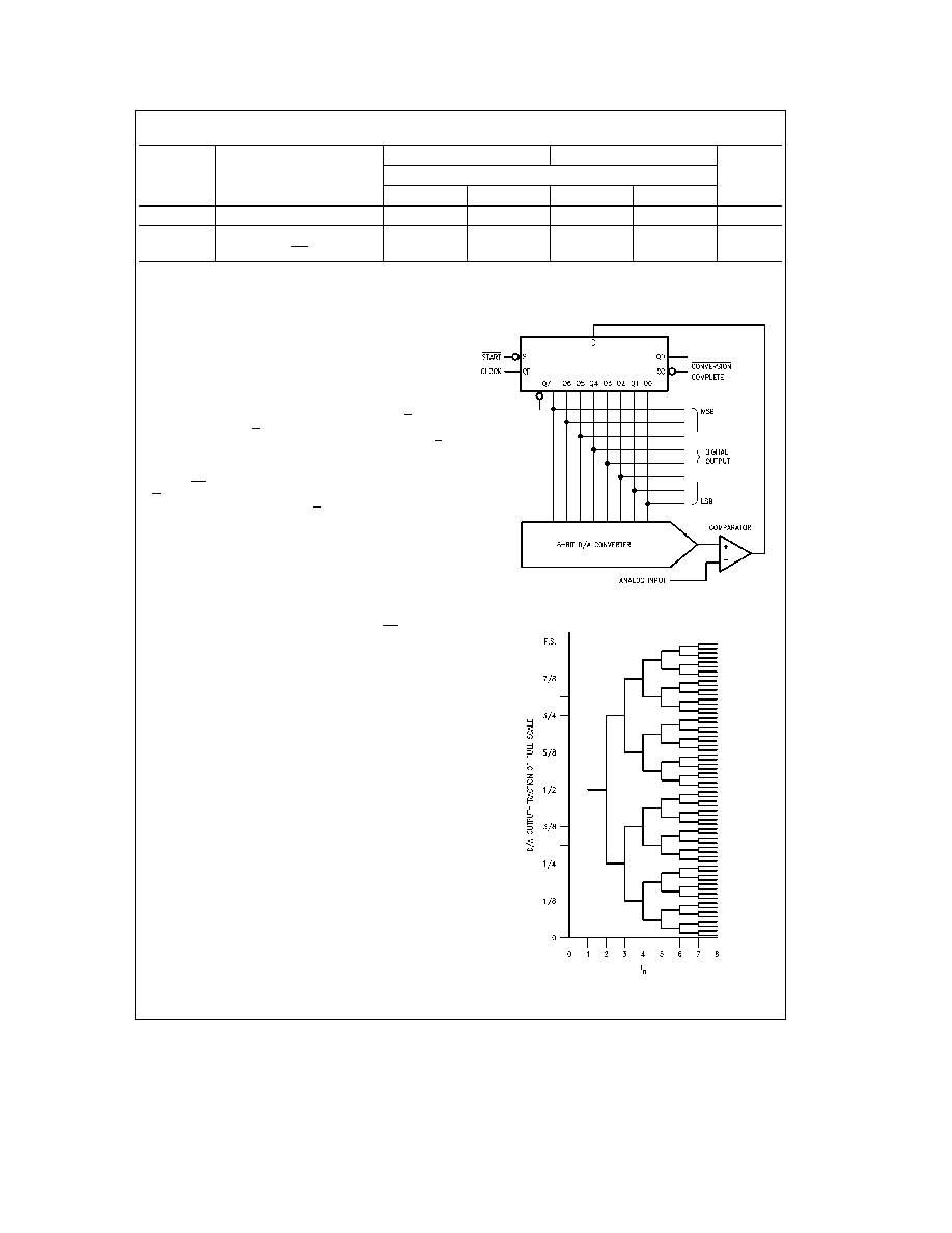
Functional Description
The register stages are composed of transparent RS latch-
es arranged in master slave pairs The master and slave
latches are enabled separately by non-overlapping comple-
mentary signals w1 and w2 derived internally from the CP
input Master latches are enabled when CP is LOW and
slave latches are enabled when CP is HIGH Information is
transferred from master to slave and thus to the outputs by
the LOW-to-HIGH transition of CP
Initializing the register requires a LOW signal on S while
exercising CP With S and CP LOW all master latches are
SET (Q side HIGH) A LOW-to-HIGH CP transition with S
remaining LOW then forces the slave latches to the condi-
tion wherein Q7 is LOW and all other register outputs in-
cluding CC are HIGH This condition will prevail as long as
S remains LOW regardless of subsequent CP rising edge
To start the conversion process S must return to the HIGH
state On the next CP rising edge the information stored in
the serial data input latch is transferred to Q
D
and Q7 while
Q6 is forced to the LOW state On the rising edge of the
next seven clocks this LOW signal is shifted downstream
one bit at a time while the serial data enters the register
position one bit behind this LOW signal as shown in the
Truth Table Note that after a serial data bit appears at a
particular output that register position undergoes no further
changes After the shifted LOW signal reaches CC the reg-
ister is locked up and no further changes can occur until the
register is initialized for the next conversion process
Figure a shows a simplified hook-up of a LS502 a D A con-
verter and a comparator arranged to convert an analog in-
put voltage into an 8-bit binary number by the successive
approximation technique
Figure b is an idealized graph
showing the various values that the D A converter output
voltage can assume in the course of the conversion The
vertical axis is calibrated in fractions of the full-scale output
capability of the D A converter and the horizontal axis rep-
resents the successive states of the Truth Table At time t1
Q7 is LOW and Q6 ≠ Q0 are HIGH causing the D A output
to be one-half of full scale If the analog input voltage is
greater than this voltage the comparator output (hence the
D input of the LS502) will be LOW and at times t2 the D A
output will rise to three-fourths of full scale because Q7 will
remain LOW and contribute 50% while Q6 is forced LOW
and contributes another 25% On the other hand if the ana-
log input voltage is less than one-half of full scale the com-
parator output will be HIGH and Q7 will go HIGH at t2 Q6
will still be forced LOW at t2 and the D A output will de-
crease to 25% of full scale Thus with each successive
clock the D A output will change by smaller increments
When the conversion is completed at t9 the binary number
represented by the register outputs will be the numerator of
the fraction n 256 representing the analog input voltage as
a fraction of the full scale output D A converter
TL F 10189 ≠ 4
FIGURE a
TL F 10189 ≠ 5
FIGURE b
3
Truth Table
Time
Inputs
Outputs
t
n
D
S
Q
D
Q7
Q6
Q5
Q4
Q3
Q2
Q1
Q0
CC
0
X
L
X
X
X
X
X
X
X
X
X
X
1
D7
H
X
L
H
H
H
H
H
H
H
H
2
D6
H
D7
D7
L
H
H
H
H
H
H
H
3
D6
H
D6
D7
D6
L
H
H
H
H
H
H
4
D4
H
D5
D7
D6
D5
L
H
H
H
H
H
5
D3
H
D4
D7
D6
D5
D4
L
H
H
H
H
6
D2
H
D3
D7
D6
D5
D4
D3
L
H
H
H
7
D1
H
D2
D7
D6
D5
D4
D3
D2
L
H
H
8
D0
H
D1
D7
D6
D5
D4
D3
D2
D1
L
H
9
X
H
D0
D7
D6
D5
D4
D3
D2
D1
D0
L
10
X
H
X
D7
D6
D5
D4
D3
D2
D1
D0
L
H
e
HIGH Voltage Level
L
e
LOW Voltage Level
X
e
Immaterial
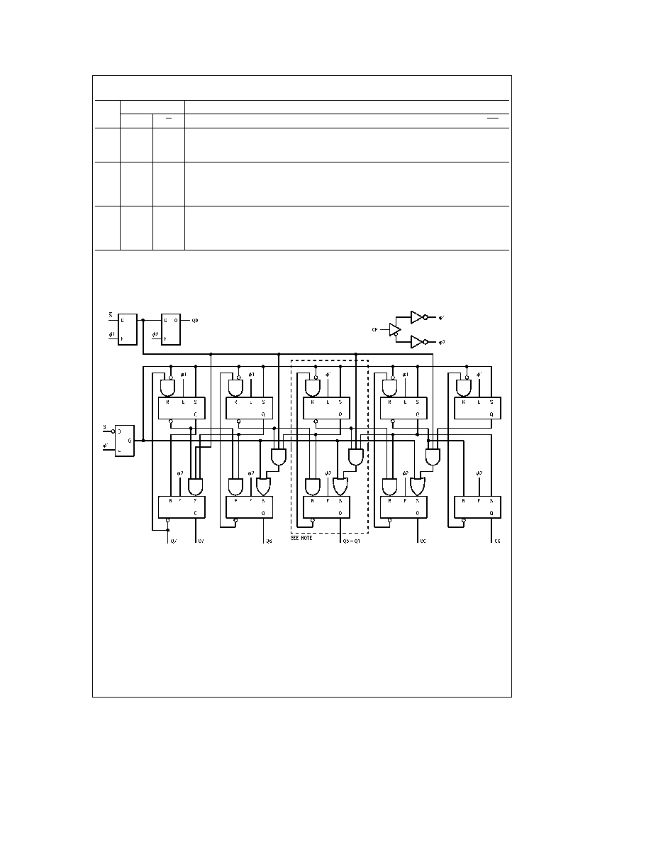
Logic Diagram
TL F 10189 ≠ 3
Note
Cell logic is repeated for register stages Q5 to Q1
4
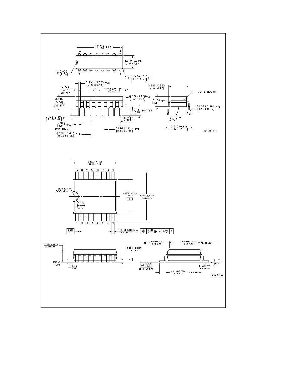
Physical Dimensions
inches (millimeters)
16-Lead Ceramic Dual-In-Line Package (J)
Order Number DM54LS502J
NS Package Number J16A
16-Lead Wide Small Outline Molded Package (M)
Order Number DM74LS502WM
NS Package Number M16B
5