DS26C31T/DS26C31M
CMOS Quad TRI-STATE
Æ
Differential Line Driver
General Description
The DS26C31 is a quad differential line driver designed for
digital
data
transmission
over
balanced
lines.
The
DS26C31T meets all the requirements of EIA standard
RS-422 while retaining the low power characteristics of
CMOS. The DS26C31M is compatible with EIA standard
RS-422; however, one exception in test methodology is
taken (Note 8). This enables the construction of serial and
terminal interfaces while maintaining minimal power con-
sumption.
The DS26C31 accepts TTL or CMOS input levels and trans-
lates these to RS-422 output levels. This part uses special
output circuitry that enables the drivers to power down with-
out loading down the bus. This device has enable and dis-
able circuitry common to all four drivers. The DS26C31 is pin
compatible to the AM26LS31 and the DS26LS31.
All inputs are protected against damage due to electrostatic
discharge by diodes to V
CC
and ground.
Features
n
TTL input compatible
n
Typical propagation delays: 6 ns
n
Typical output skew: 0.5 ns
n
Outputs will not load line when V
CC
= 0V
n
DS26C31T meets the requirements of EIA standard
RS-422
n
Operation from single 5V supply
n
TRI-STATE outputs for connection to system buses
n
Low quiescent current
n
Available in surface mount
n
Mil-Std-883C compliant
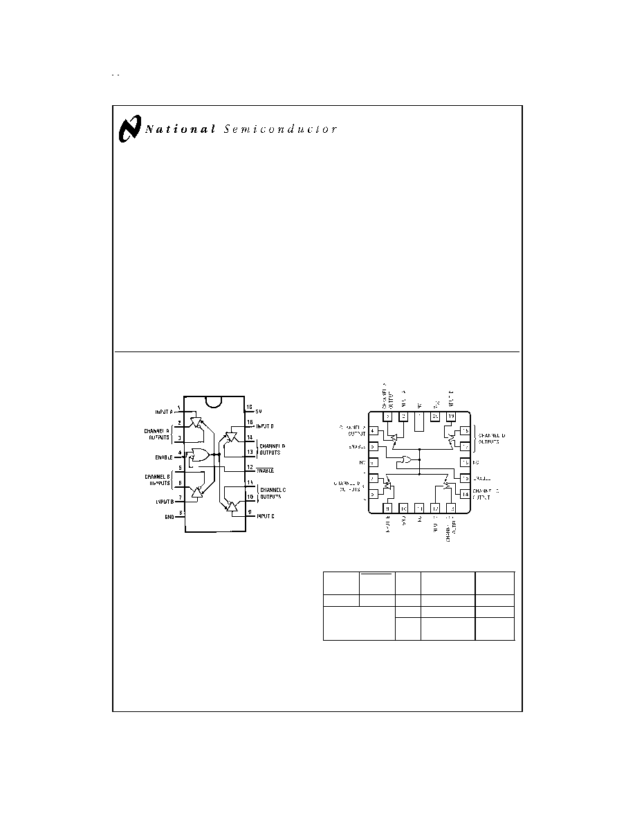
Connection Diagrams
Truth Table
ENABLE ENABLE
Input
Non-Inverting
Inverting
Output
Output
L
H
X
Z
Z
All other
L
L
H
combinations of
H
H
L
enable inputs
L = Low logic state
X = Irrelevant
H = High logic state
Z = TRI-STATE (high impedance)
TRI-STATE
Æ
is a registered trademark of National Semiconductor Corporation.
FACT
TM
is a trademark of National Semiconductor Corporation.
Dual-In-Line Package
DS008574-1
Top View
Order Number DS26C31TM or DS26C31TN
See NS Package Number M16A or N16E
For Complete Military Product Specifications,
refer to the appropriate SMD or MDS.
Order Number DS26C31ME/883, DS26C31MJ/883
or DS26C31MW/883
See NS Package Number E20A, J16A or W16A
20-Lead Ceramic Leadless Chip Carrier (E)
DS008574-12
June 1998
DS26C31T/DS26C31M
CMOS
Quad
TRI-ST
A
T
E
Differential
Line
Driver
© 1998 National Semiconductor Corporation
DS008574
www.national.com
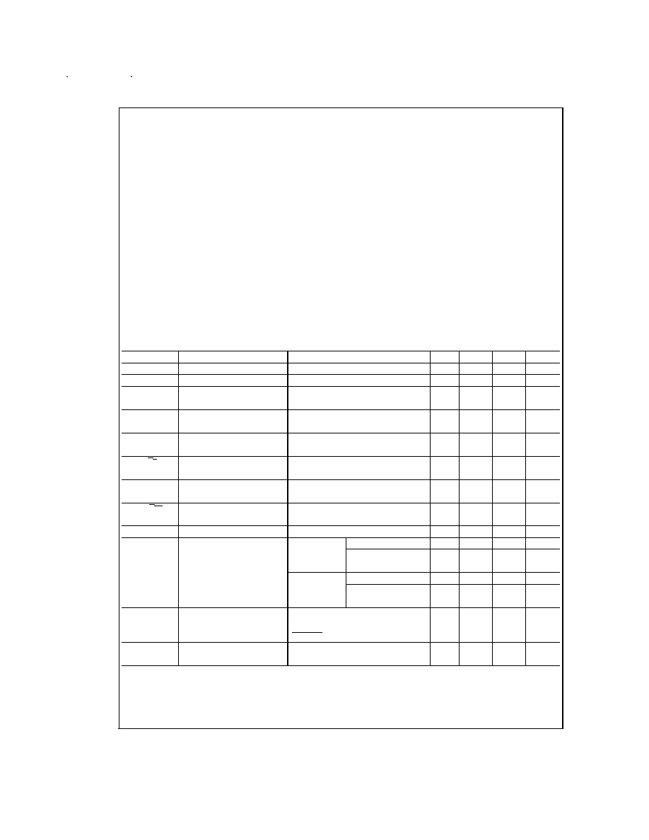
Absolute Maximum Ratings
(Notes 1, 2)
If Military/Aerospace specified devices are required,
please contact the National Semiconductor Sales Office/
Distributors for availability and specifications.
Supply Voltage (V
CC
)
-0.5V to 7.0V
DC Input Voltage (V
IN
)
-1.5V to V
CC
+1.5V
DC Output Voltage (V
OUT
)
-0.5V to 7V
Clamp Diode Current (I
IK
, I
OK
)
±
20 mA
DC Output Current, per pin (I
OUT
)
±
150 mA
DC V
CC
or GND Current,
per pin (I
CC
)
±
150 mA
Storage Temperature Range (T
STG
)
-65∞C to +150∞C
Max. Power Dissipation (P
D
)
@
25∞C (Note 3)
Ceramic "J" Pkg.
2419 mW
Plastic "N" Pkg.
1736 mW
SOIC "M" Pkg.
1226 mW
Ceramic "W" Pkg.
1182 mW
Ceramic "E" Pkg.
2134 mW
Lead Temperature (T
L
)
(Soldering, 4 sec.)
260∞C
This device does not meet 2000V ESD Rating. (Note 13)
Operating Conditions
Min
Max
Units
Supply Voltage (V
CC
)
4.50
5.50
V
DC Input or Output Voltage
(V
IN
, V
OUT
)
0
V
CC
V
Operating Temperature Range (T
A
)
DS26C31T
-40
+85
∞C
DS26C31M
-55
+125
∞C
Input Rise or Fall Times (t
r
, t
f
)
500
ns
DC Electrical Characteristics
V
CC
= 5V
±
10% (unless otherwise specified) (Note 4)
Symbol
Parameter
Conditions
Min
Typ
Max
Units
V
IH
High Level Input Voltage
2.0
V
V
IL
Low Level Input Voltage
0.8
V
V
OH
High Level Output Voltage
V
IN
= V
IH
or V
IL
,
2.5
3.4
V
I
OUT
= -20 mA
V
OL
Low Level Output
V
IN
= V
IH
or V
IL
,
0.3
0.5
V
Voltage
I
OUT
= 20 mA
V
T
Differential Output
R
L
= 100
2.0
3.1
V
Voltage
(Note 5)
|V
T
| - |V
T
|
Difference In
R
L
= 100
0.4
V
Differential Output
(Note 5)
V
OS
Common Mode
R
L
= 100
1.8
3.0
V
Output Voltage
(Note 5)
|V
OS
- V
OS
|
Difference In
R
L
= 100
0.4
V
Common Mode Output
(Note 5)
I
IN
Input Current
V
IN
= V
CC
, GND, V
IH
, or V
IL
±
1.0
µA
I
CC
Quiescent Supply
DS26C31T
V
IN
= V
CC
or GND
200
500
µA
Current (Note 6)
I
OUT
= 0 µA
V
IN
= 2.4V or 0.5V
0.8
2.0
mA
(Note 6)
DS26C31M
V
IN
= V
CC
or GND
200
500
µA
I
OUT
= 0 µA
V
IN
= 2.4V or 0.5V
0.8
2.1
mA
(Note 6)
I
OZ
TRI-STATE Output
V
OUT
= V
CC
or GND
Leakage Current
ENABLE = V
IL
±
0.5
±
5.0
µA
ENABLE = V
IH
I
SC
Output Short
V
IN
= V
CC
or GND
-30
-150
mA
Circuit Current
(Notes 5, 7)
www.national.com
2
DC Electrical Characteristics
(Continued)
V
CC
= 5V
±
10% (unless otherwise specified) (Note 4)
Symbol
Parameter
Conditions
Min
Typ
Max
Units
I
OFF
Output Leakage Current
DS26C31T
V
OUT
= 6V
100
µA
Power Off (Note 5)
V
CC
= 0V
V
OUT
= -0.25V
-100
µA
DS26C31M
V
OUT
= 6V
100
µA
V
CC
= 0V
V
OUT
= 0V
-100
µA
(Note 8)
Note 1: Absolute Maximum Ratings are those values beyond which the safety of the device cannot be guaranteed. They are not meant to imply that the device
should be operated at these limits. The table of "Electrical Characteristics" provide conditions for actual device operation.
Note 2: Unless otherwise specified, all voltages are referenced to ground. All currents into device pins are positive, all currents out of device pins are negative.
Note 3: Ratings apply to ambient temperature at 25∞C. Above this temperature derate N package at 13.89 mW/∞C, J package 16.13 mW/∞C, M package 9.80 mW/∞C,
E package 12.20 mW/∞C, and W package 6.75 mW/∞C.
Note 4: Unless otherwise specified, min/max limits apply across the recommended operating temperature range. All typicals are given for V
CC
= 5V and T
A
= 25∞C.
Note 5: See EIA Specification RS-422 for exact test conditions.
Note 6: Measured per input. All other inputs at V
CC
or GND.
Note 7: This is the current sourced when a high output is shorted to ground. Only one output at a time should be shorted.
Note 8: The DS26C31M (-55∞C to +125∞C) is tested with V
OUT
between +6V and 0V while RS-422A condition is +6V and -0.25V.
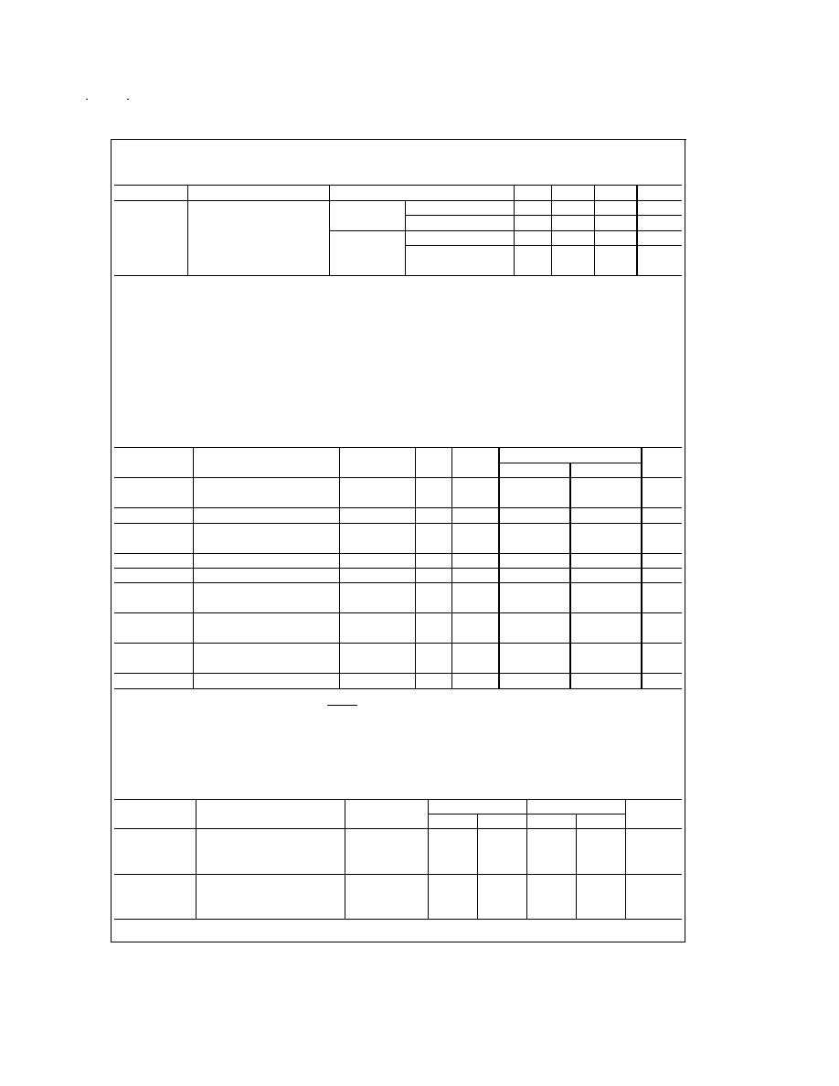
Switching Characteristics
V
CC
= 5V
±
10%, t
r
6 ns, t
f
6 ns (
Figures 1, 2, 3, 4) (Note 4)
Symbol
Parameter
Conditions
Min
Typ
Max
Units
DS26C31T
CS26C31M
t
PLH
, t
PHL
Propagation Delays
S1 Open
2
6
11
14
ns
Input to Output
Skew
(Note 9)
S1 Open
0.5
2.0
3.0
ns
t
TLH
, t
THL
Differential Output Rise
S1 Open
6
10
14
ns
And Fall Times
t
PZH
Output Enable Time
S1 Closed
11
19
22
ns
t
PZL
Output Enable Time
S1 Closed
13
21
28
ns
t
PHZ
Output Disable Time
S1 Closed
5
9
12
ns
(Note 10)
t
PLZ
Output Disable Time
S1 Closed
7
11
14
ns
(Note 10)
C
PD
Power Dissipation
50
pF
Capacitance (Note 11)
C
IN
Input Capacitance
6
pF
Note 9: Skew is defined as the difference in propagation delays between complementary outputs at the 50% point.
Note 10: Output disable time is the delay from ENABLE or ENABLE being switched to the output transistors turning off. The actual disable times are less than in-
dicated due to the delay added by the RC time constant of the load.
Note 11: C
PD
determines the no load dynamic power consumption, P
D
= C
PD
V
CC
2 f + I
CC
V
CC
, and the no load dynamic current consumption, I
S
= C
PD
V
CC
f +
I
CC
.
Comparison Table of Switching Characteristics into "LS-Type" Load
V
CC
= 5V, T
A
= 25∞C, t
r
6 ns, t
f
6 ns (
Figures 2, 4, 5, 6) (Note 12)
Symbol
Parameter
Conditions
DS26C31T
DS26LS31C
Units
Typ
Max
Typ
Max
t
PLH
, t
PHL
Propagation Delays
C
L
= 30 pF
Input to Output
S1 Closed
6
8
10
15
ns
S2 Closed
Skew
(Note 9)
C
L
= 30 pF
S1 Closed
0.5
1.0
2.0
6.0
ns
S2 Closed
www.national.com
3
Comparison Table of Switching Characteristics into "LS-Type" Load
(Continued)
V
CC
= 5V, T
A
= 25∞C, t
r
6 ns, t
f
6 ns (
Figures 2, 4, 5, 6) (Note 12)
Symbol
Parameter
Conditions
DS26C31T
DS26LS31C
Units
Typ
Max
Typ
Max
t
THL
, t
TLH
Differential Output Rise
C
L
= 30 pF
and Fall Times
S1 Closed
4
6
ns
S2 Closed
t
PLZ
Output Disable Time
C
L
= 10 pF
(Note 10)
S1 Closed
6
9
15
35
ns
S2 Open
t
PHZ
Output Disable Time
C
L
= 10 pF
(Note 10)
S1 Open
4
7
15
25
ns
S2 Closed
t
PZL
Output Enable Time
C
L
= 30 pF
S1 Closed
14
20
20
30
ns
S2 Open
t
PZH
Output Enable Time
C
L
= 30 pF
S1 Open
11
17
20
30
ns
S2 Closed
Note 12: This table is provided for comparison purposes only. The values in this table for the DS26C31 reflect the performance of the device but are not tested or
guaranteed.
Note 13: ESD Rating:
HBM (1.5 k
, 100 pF)
Inputs
1500V
Outputs
1000V
EIAJ (0
, 200 pF)
350V
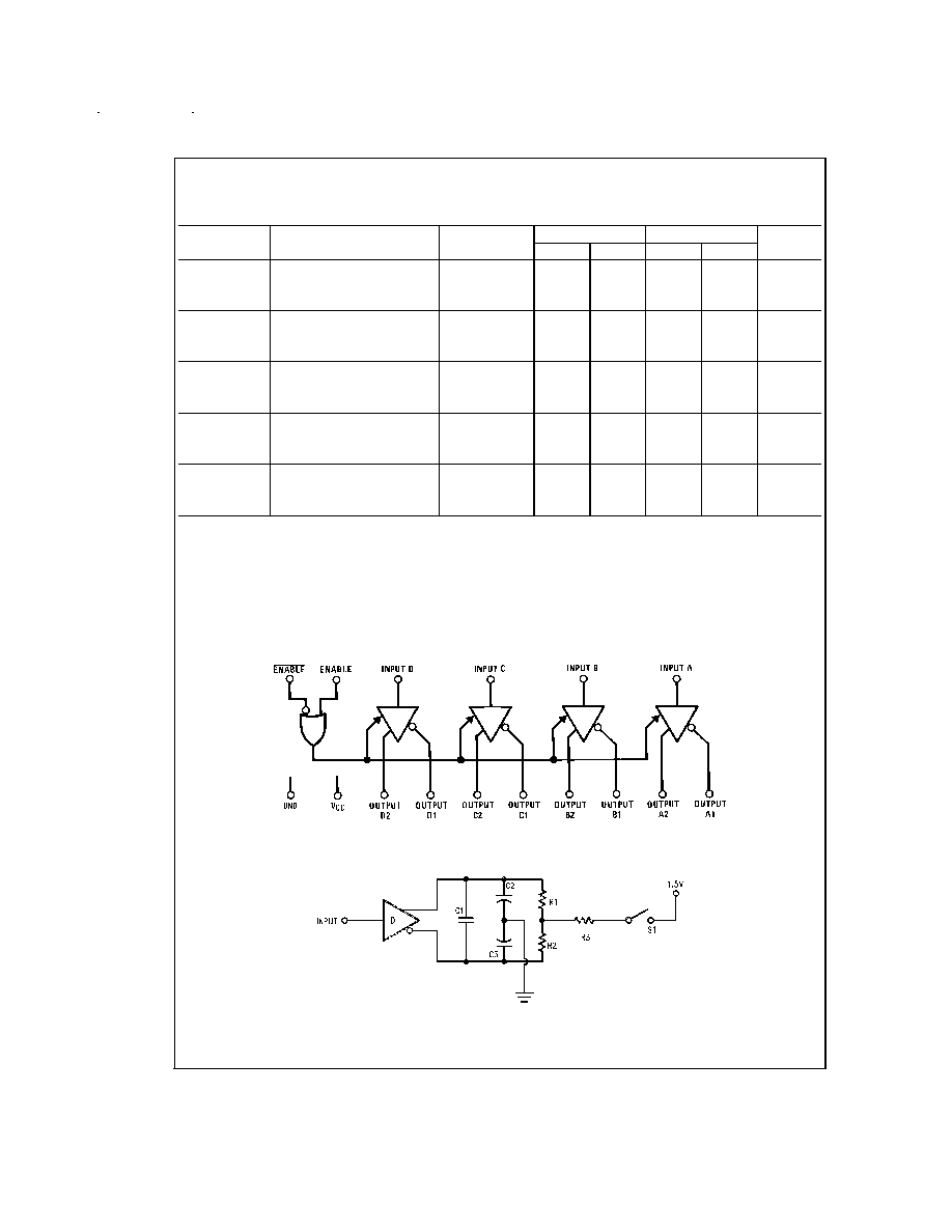
Logic Diagram
AC Test Circuit and Switching Time Waveforms
DS008574-2
DS008574-3
Note: C1 = C2 = C3 = 40 pF (Including Probe and Jig Capacitance), R1 = R2 = 50
, R3 = 500
.
FIGURE 1. AC Test Circuit
www.national.com
4
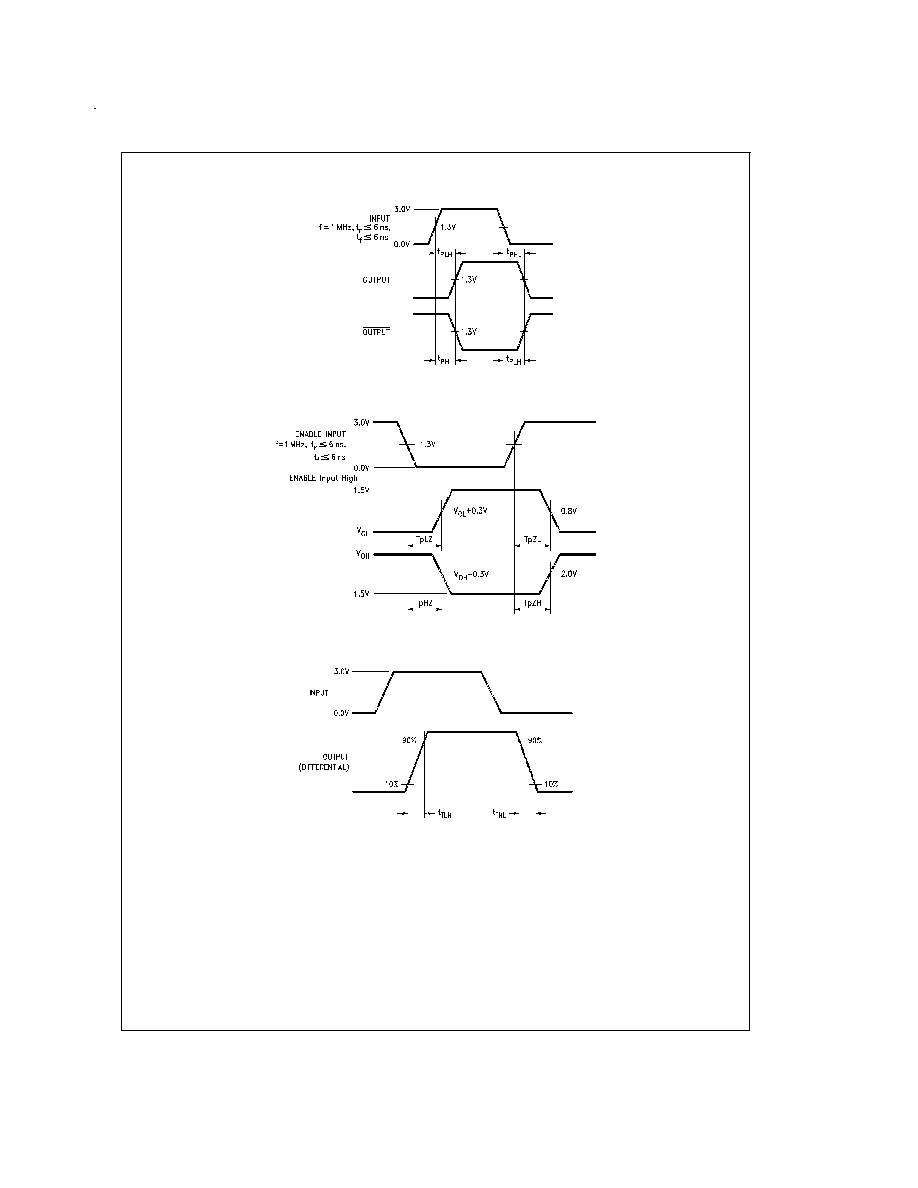
AC Test Circuit and Switching Time Waveforms
(Continued)
DS008574-4
FIGURE 2. Propagation Delays
DS008574-5
FIGURE 3. Enable and Disable Times
DS008574-7
Input pulse; f = 1 MHz, 50%; t
r
6 ns, t
f
6 ns
FIGURE 4. Differential Rise and Fall Times
www.national.com
5