54ACTQ241
Quiet Series Octal Buffer/Line Driver with TRI-STATE
Æ
Outputs
General Description
The ACTQ241 is an octal buffer and line driver designed to
be employed as a memory address driver, clock driver and
bus oriented transmitter or receiver which provides improved
PC board density. The ACTQ utilizes NSC Quiet Series tech-
nology to guarantee quiet output switching and improved dy-
namic threshold performance. FACT Quiet Series
TM
features
GTO
TM
output control and undershoot corrector in addition to
a split ground bus for superior performance.
Features
n
I
CC
and I
OZ
reduced by 50%
n
Guaranteed simultaneous switching noise level and
dynamic threshold performance
n
Improved latch-up immunity
n
TRI-STATE outputs drive bus lines or buffer memory
address registers
n
Outputs source/sink 24 mA
n
Faster prop delays than the standard 'AC/'ACT241
n
4 kV minimum ESD immunity ('ACTQ)
n
Standard Microcircuit Drawing (SMD) 5962-92185
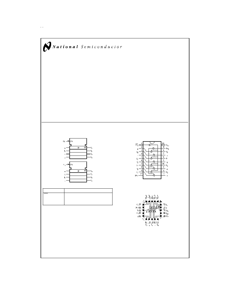
Logic Symbol
Pin Names
Description
OE
1
, OE
2
TRI-STATE Output Enable Inputs
I
0
≠I
7
Inputs
O
0
≠O
7
Outputs
Connection Diagrams
GTO
TM
is a trademark of National Semiconductor Corporation.
TRI-STATE
Æ
is a registered trademark of National Semiconductor Corporation.
FACT
Æ
is a registered trademark of Fairchild Semiconductor Corporation.
FACT Quiet Series
TM
is a trademark of Fairchild Semiconductor Corporation.
IEEE/IEC
DS100246-1
Pin Assignment
for DIP and Flatpak
DS100246-2
Pin Assignment
for LCC
DS100246-3
August 1998
54ACTQ241
Quiet
Series
Octal
Buffer/Line
Driver
with
TRI-ST
A
T
E
Outputs
© 1998 National Semiconductor Corporation
DS100246
www.national.com

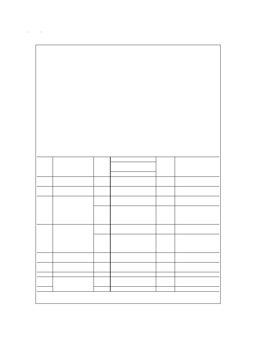
Truth Tables
Inputs
Outputs
OE
1
I
n
(Pins 12, 14, 16, 18)
L
L
L
L
H
H
H
X
Z
Inputs
Outputs
OE
2
I
n
(Pins 3, 5, 7, 9)
H
L
L
H
H
H
H
X
Z
H = HIGH Voltage Level
L = LOW Voltage Level
X = Immaterial
Z = High Impedance
www.national.com
2
Absolute Maximum Ratings
(Note 1)
If Military/Aerospace specified devices are required,
please contact the National Semiconductor Sales Office/
Distributors for availability and specifications.
Supply Voltage (V
CC
)
-0.5V to +7.0V
DC Input Diode Current (I
IK
)
V
I
= -0.5V
-20 mA
V
I
= V
CC
+ 0.5V
+20 mA
DC Input Voltage (V
I
)
-0.5V to V
CC
+ 0.5V
DC Output Diode Current (I
OK
)
V
O
= -0.5V
-20 mA
V
O
= V
CC
+ 0.5V
+20 mA
DC Output Voltage (V
O
)
-0.5V to V
CC
+ 0.5V
DC Output Source
or Sink Current (I
O
)
±
50 mA
DC V
CC
or Ground Current
per Output Pin (I
CC
or I
GND
)
±
50 mA
Storage Temperature (T
STG
)
-65∞C to +150∞C
DC Latch-Up Source or
Sink Current
±
300 mA
Junction Temperature (T
J
)
CDIP
175∞C
Recommended Operating
Conditions
Supply Voltage (V
CC
)
'ACTQ
4.5V to 5.5V
Input Voltage (V
I
)
0V to V
CC
Output Voltage (V
O
)
0V to V
CC
Operating Temperature (T
A
)
54ACTQ
-55∞C to +125∞C
Minimum Input Edge Rate
V/
t
'ACTQ Devices
V
IN
from 0.8V to 2.0V
V
CC
@
4.5V, 5.5V
125 mV/ns
Note 1: Absolute maximum ratings are those values beyond which damage
to the device may occur. The databook specifications should be met, without
exception, to ensure that the system design is reliable over its power supply,
temperature, and output/input loading variables. National does not recom-
mend operation of FACT
Æ
circuits outside databook specifications.
Note 2: All commercial packaging is not recommended for applications re-
quiring greater than 2000 temperature cycles from -40∞C to +125∞C.
DC Electrical Characteristics for 'ACTQ Family Devices
54ACTQ
Symbol
Parameter
V
CC
T
A
=
Units
Conditions
(V)
-55∞C to +125∞C
Guaranteed Limits
V
IH
Minimum High Level
4.5
2.0
V
V
OUT
= 0.1V
Input Voltage
5.5
2.0
or V
CC
- 0.1V
V
IL
Maximum Low Level
4.5
0.8
V
V
OUT
= 0.1V
Input Voltage
5.5
0.8
or V
CC
- 0.1V
V
OH
Minimum High Level
4.5
4.4
V
I
OUT
= -50 µA
Output Voltage
5.5
5.4
(Note 3)
V
IN
= V
IL
or V
IH
4.5
3.70
V
I
OH
= -24 mA
5.5
4.70
I
OH
= -24 mA
V
OL
Maximum Low Level
4.5
0.1
V
I
OUT
= 50 µA
Output Voltage
5.5
0.1
(Note 3)
V
IN
= V
IL
or V
IH
4.5
0.50
V
I
OL
= 24 mA
5.5
0.50
I
OL
= 24 mA
I
IN
Maximum Input
5.5
±
1.0
µA
V
I
= V
CC
, GND
Leakage Current
I
OZ
Maximum TRI-STATE
5.5
±
5.0
µA
V
I
= V
IL
, V
IH
Leakage Current
V
O
= V
CC
, GND
I
CCT
Maximum I
CC
/Input
5.5
1.6
mA
V
I
= V
CC
- 2.1V
(Note 4)
Minimum Dynamic
Output Current
I
OLD
5.5
50
mA
V
OLD
= 1.65V Max
I
OHD
5.5
-50
mA
V
OHD
= 3.85V Min
www.national.com
3
DC Electrical Characteristics for 'ACTQ Family Devices
(Continued)
54ACTQ
Symbol
Parameter
V
CC
T
A
=
Units
Conditions
(V)
-55∞C to +125∞C
Guaranteed Limits
I
CC
Maximum Quiescent
5.5
80.0
µA
V
IN
= V
CC
Supply Current
or GND (Note 5)
V
OLP
Quiet Output
5.0
1.5
V
Maximum Dynamic V
OL
(Notes 6, 7)
V
OLV
Quiet Output
5.0
-1.2
V
Minimum Dynamic V
OL
(Notes 6, 7)
Note 3: All outputs loaded; thresholds on input associated with output under test.
Note 4: Maximum test duration 2.0 ms, one output loaded at a time.
Note 5: I
CC
for 54ACTQ
@
25∞C is identical to 74ACTQ
@
25∞C.
Note 6: Plastic DIP package.
Note 7: Max number of outputs defined as (n). Data Inputs are driven 0V to 3V. One output
@
GND.
Note 8: Max number of Data Inputs (n) switching. n-1 Inputs switching 0V to 3V ('ACTQ). Input-under-test switching: 3V to threshold (V
ILD
), 0V to threshold (V
IHD
),
f = 1 MHz.
AC Electrical Characteristics
54ACTQ
V
CC
T
A
= -55∞C
Fig.
Symbol
Parameter
(V)
to +125∞C
Units
No.
(Note 9)
C
L
= 50 pF
Min
Max
t
PHL
, t
PLH
Propagation Delay
5.0
1.5
8.0
ns
Figure 4
Data to Output
t
PZL
, t
PZH
Output Enable Time
5.0
1.5
10.5
ns
Figure 5
t
PHZ
, t
PLZ
Output Disable Time
5.0
1.5
9.5
ns
Figure 5
Note 9: Voltage Range 5.0 is 5.0V
±
0.5V.
Note 10: Skew is defined as the absolute value of the difference between the actual propagation delay for any two separate outputs of the same device. The speci-
fication applies to any outputs switching in the same direction, either HIGH to LOW (t
OSHL
) or LOW to HIGH (t
OSLH
). Parameter guaranteed by design.
Capacitance
Symbol
Parameter
Typ
Units
Conditions
C
IN
Input Capacitance
4.5
pF
V
CC
= OPEN
C
PD
Power Dissipation
70
pF
V
CC
= 5.0V
Capacitance
www.national.com
4
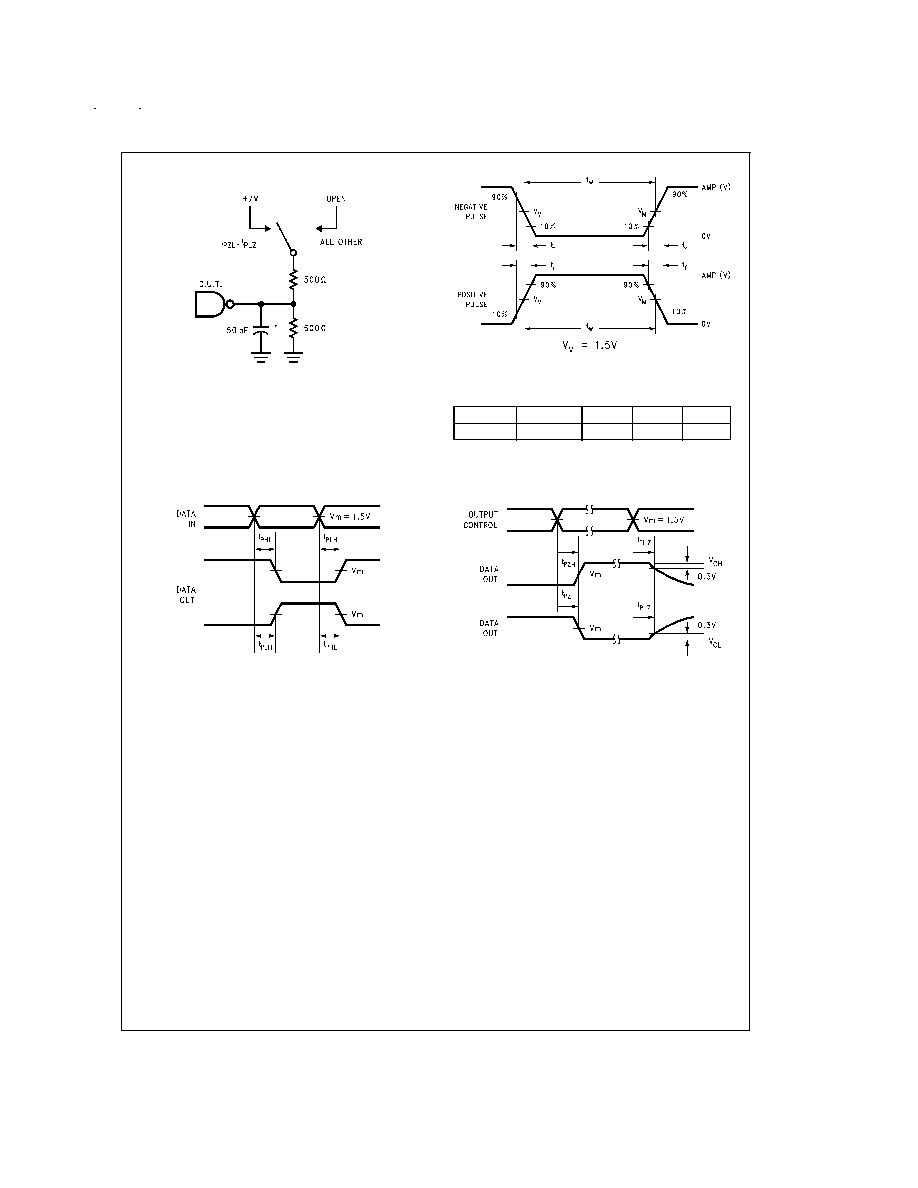
AC Loading
AC Waveforms
DS100246-7
*Includes jig and probe capacitance
FIGURE 1. Standard AC Test Load
DS100246-8
FIGURE 2. Test Input Signal Levels
Amplitude
Rep. Rate
t
w
t
r
t
f
3.0V
1 MHz
500 ns
2.5 ns
2.5 ns
FIGURE 3. Test Input Signal Requirements
DS100246-9
FIGURE 4. Propagation Delay Waveforms for
Inverting and Non-Inverting Functions
DS100246-10
FIGURE 5. TRI-STATE Output HIGH and LOW
Enable and Disable Time
www.national.com
5