54ABT646
Octal Transceivers and Registers with TRI-STATE
Æ
Outputs
General Description
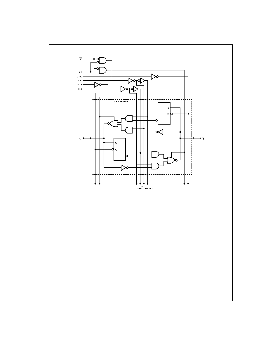
The 'ABT646 consists of bus transceiver circuits with
TRI-STATE, D-type flip-flops, and control circuitry arranged
for multiplexed transmission of data directly from the input
bus or from the internal registers. Data on the A or B bus will
be clocked into the registers as the appropriate clock pin
goes to a high logic level. Control OE and direction pins are
provided to control the transceiver function. In the trans-
ceiver mode, data present at the high impedance port may
be stored in either the A or the B register or in both. The se-
lect controls can multiplex stored and real-time (transparent
mode) data. The direction control determines which bus will
receive data when the enable control OE is Active LOW. In
the isolation mode (control OE HIGH), A data may be stored
in the B register and/or B data may be stored in the A regis-
ter.
Features
n
Independent registers for A and B buses
n
Multiplexed real-time and stored data
n
A and B output sink capability of 48 mA, source
capability of 24 mA
n
Guaranteed multiple output switching specifications
n
Output switching specified for both 50 pF and 250 pF
loads
n
Guaranteed simultaneous switching noise level and
dynamic threshold performance
n
Guaranteed latchup protection
n
High impedance glitch free bus loading during entire
power up and power down cycle
n
Nondestructive hot insertion capability
n
Standard Microcircuit Drawing (SMD) 5962-9457701
Ordering Code
Military
Package Number
Package Description
54ABT646J-QML
J24A
24-Lead Ceramic Dual-In-Line
54ABT646W-QML
W24C
24-Lead Cerpack
54ABT646E-QML
E28A
28-Lead Ceramic Leadless Chip Carrier, Type C
TRI-STATE
Æ
is a registered trademark of National Semiconductor Corporation.
July 1998
54ABT646
Octal
T
ransceivers
and
Registers
with
TRI-ST
A
T
E
Outputs
© 1998 National Semiconductor Corporation
DS100209
www.national.com

Connection Diagrams
(Continued)
Inputs
Data I/O
(Note 1)
Function
OE
DIR
CPAB
CPBA
SAB SBA A
0
≠A
7
B
0
≠B
7
H
X
H or L
H or L
X
X
Isolation
H
X
N
X
X
X
Input
Input
Clock A
n
Data into A Register
H
X
X
N
X
X
Clock B
n
Data into B Register
L
H
X
X
L
X
A
n
to B
n
-- Real Time (Transparent Mode)
L
H
N
X
L
X
Input
Output
Clock A
n
Data into A Register
L
H
H or L
X
H
X
A Register to B
n
(Stored Mode)
L
H
N
X
H
X
Clock A
n
Data into A Register and Output to B
n
L
L
X
X
X
L
B
n
to A
n
-- Real Time (Transparent Mode)
L
L
X
N
X
L
Output
Input
Clock B
n
Data into B Register
L
L
X
H or L
X
H
B Register to A
n
(Stored Mode)
L
L
X
N
X
H
Clock B
n
Data into B Register and Output to A
n
H = HIGH Voltage Level
L = LOW Voltage Level
X = Immaterial
N
= LOW-to-HIGH Transition
Note 1: The data output functions may be enabled or disabled by various signals at the OE and DIR inputs. Data input functions are always enabled; i.e., data at
the bus pins will be stored on every LOW-to-HIGH transition of the appropriate clock inputs.
Real Time Transfer
A-Bus to B-Bus
DS100209-5
FIGURE 1.
Real Time Transfer
B-Bus to A-Bus
DS100209-6
FIGURE 2.
Storage from
Bus to Register
DS100209-7
FIGURE 3.
Transfer from
Register to Bus
DS100209-8
FIGURE 4.
3
www.national.com

Absolute Maximum Ratings
(Note 2)
If Military/Aerospace specified devices are required,
please contact the National Semiconductor Sales Office/
Distributors for availability and specifications.
Storage Temperature
-65∞C to +150∞C
Ambient Temperature under Bias
-55∞C to +125∞C
Junction Temperature under Bias
Ceramic
-55∞C to +175∞C
V
CC
Pin Potential to Ground Pin
-0.5V to +7.0V
Input Voltage (Note 3)
-0.5V to +7.0V
Input Current (Note 3)
-30 mA to +5.0 mA
Voltage Applied to Any Output
in the Disable or
Power-Off State
-0.5V to +5.5V
in the HIGH State
-0.5V to V
CC
Current Applied to Output
in LOW State (Max)
twice the rated I
OL
(mA)
DC Latchup Source Current
-500 mA
Over Voltage Latchup (I/O)
10V
Recommended Operating
Conditions
Free Air Ambient Temperature
Military
-55∞C to +125∞C
Supply Voltage
Military
+4.5V to +5.5V
Minimum Input Edge Rate
(
V/
t)
Data Input
50 mV/ns
Enable Input
20 mV/ns
Clock Input
100 mV/ns
Note 2: Absolute maximum ratings are values beyond which the device may
be damaged or have its useful life impaired. Functional operation under these
conditions is not implied.
Note 3: Either voltage limit or current limit is sufficient to protect inputs.
DC Electrical Characteristics
Symbol
Parameter
ABT646
Units
V
CC
Conditions
Min Typ
Max
V
IH
Input HIGH Voltage
2.0
V
Recognized HIGH Signal
V
IL
Input LOW Voltage
0.8
V
Recognized LOW Signal
V
CD
Input Clamp Diode Voltage
-1.2
V
Min
I
IN
= -18 mA (Non I/O Pins)
V
OH
Output HIGH
Voltage
54ABT
2.5
V
I
OH
= -3 mA, (A
n
, B
n
)
54ABT
2.0
Min
I
OH
= -24 mA, (A
n
, B
n
)
V
OL
Output LOW
Voltage
54ABT
0.55
V
Min
I
OL
= 48 mA, (A
n
, B
n
)
V
ID
Input Leakage Test
4.75
V
0.0
I
ID
= 1.9 µA, (Non-I/O Pins)
All Other Pins Grounded
I
IH
Input HIGH Current
5
µA
Max
V
IN
= 2.7V (Non-I/O Pins) (Note 5)
5
V
IN
= V
CC
(Non-I/O Pins)
I
BVI
Input HIGH Current
Breakdown Test
7
µA
Max
V
IN
= 7.0V (Non-I/O Pins)
I
BVIT
Input HIGH Current
Breakdown Test (I/O)
100
µA
Max
V
IN
= 5.5V (A
n
, B
n
)
I
IL
Input LOW Current
-5
µA
Max
V
IN
= 0.5V (Non-I/O Pins) (Note 5)
-5
V
IN
= 0.0V (Non-I/O Pins)
I
IH
+ I
OZH
Output Leakage Current
50
µA
0V≠5.5V
V
OUT
= 2.7V (A
n
, B
n
); OE = 2.0V
I
IL
+ I
OZL
Output Leakage Current
-50
µA
0V≠5.5V
V
OUT
= 0.5V (A
n
, B
n
); OE = 2.0V
I
OS
Output Short-Circuit Current
-100
-275
mA
Max
V
OUT
= 0V (A
n
, B
n
)
I
CEX
Output HIGH Leakage Current
50
µA
Max
V
OUT
= V
CC
(A
n
, B
n
)
I
ZZ
Bus Drainage Test
100
µA
0.0V
V
OUT
= 5.5V (A
n
, B
n
);
All Others GND
I
CCH
Power Supply Current
250
µA
Max
All Outputs HIGH
I
CCL
Power Supply Current
30
mA
Max
All Outputs LOW
I
CCZ
Power Supply Current
50
µA
Max
Outputs TRI-STATE; All Others GND
I
CCT
Additional I
CC
/Input
2.5
mA
Max
V
I
= V
CC
- 2.1V
All Other Outputs at V
CC
or GND
I
CCD
Dynamic I
CC
(Note 5)
No Load
0.18
mA/MHz
Max
Outputs Open
OE and DIR = GND,
Non-I/O = GND or V
CC
(Note 4)
One Bit toggling, 50% duty cycle
5
www.national.com