
SCANPSC100F
Embedded Boundary Scan Controller
(IEEE 1149.1 Support)
General Description
The SCANPSC100F is designed to interface a generic par-
allel processor bus to a serial scan test bus. It is useful in
improving scan throughput when applying serial vectors to
system test circuitry and reduces the software overhead that
is associated with applying serial patterns with a parallel
processor. The 'PSC100F operates by serializing data from
the parallel bus for shifting through the chain of 1149.1
compliant components (i.e., scan chain). Scan data return-
ing from the scan chain is placed on the parallel port to be
read by the host processor. Up to two scan chains can be
directly controlled with the 'PSC100F via two independent
TMS pins. Scan control is supplied with user specific pat-
terns which makes the 'PSC100F protocol-independent.
Overflow and underflow conditions are prevented by stop-
ping the test clock. A 32-bit counter is used to program the
number of TCK cycles required to complete a scan operation
within the boundary scan chain or to complete a 'PSC100F
Built-In Self Test (BIST) operation. SCANPSC100F device
drivers and 1149.1 embedded test application code are
available with National's SCANEase software tools.
Features
n
Compatible with IEEE Std. 1149.1 (JTAG) Test Access
Port and Boundary Scan Architecture
n
Supported by National's SCAN Ease (Embedded
Application Software Enabler) Software
n
Uses generic, asynchronous processor interface;
compatible with a wide range of processors and PCLK
frequencies
n
Directly supports up to two 1149.1 scan chains
n
16-bit Serial Signature Compaction (SSC) at the Test
Data In (TDI) port
n
Automatically produces pseudo-random patterns at the
Test Data Out (TDO) port
n
Fabricated on FACT
TM
1.5 µm CMOS process
n
Supports 1149.1 test clock (TCK) frequencies up to
25 MHz
n
TTL-compatible inputs; full-swing CMOS outputs with
24 mA source/sink capability
n
Standard Microcircuit Drawing (SMD) 5962-9475001
Connection Diagrams
28-Pin DIP and Flatpak
Pin Assignment for LCC
10032501
10032518
FACT
TM
is a trademark of Fairchild Semiconductor Corporation.
TRI-STATE
Æ
is a registered trademark of National Semiconductor Corporation.
September 1998
SCANPSC100F
Embedded
Boundary
Scan
Controller
(IEEE
1
149.1
Support)
© 2002 National Semiconductor Corporation
DS100325
www.national.com
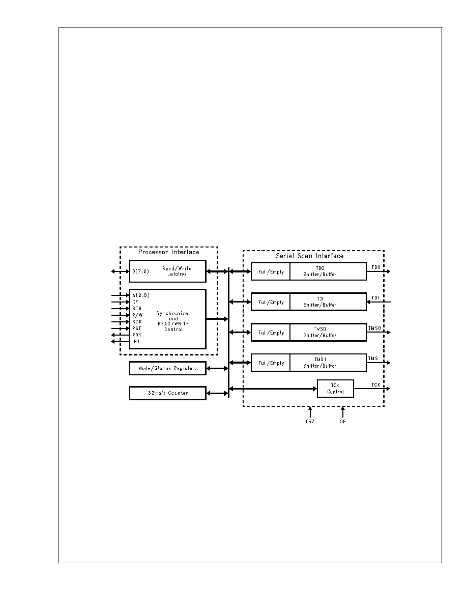
Chip Architecture
The 'PSC100 is designed to act together with a parallel bus
host as a serial test bus master. Parallel data is written by the
host to the 'PSC100, which serializes the data for application
to a serial test bus. Serial data returning from the target scan
chain(s) is placed on the processor port for parallel reads.
Several features are included in the 'PSC100 which make
scan test communication more convenient and efficient.
Figure 1 shows the major functional blocks of the 'PSC100
design. The Parallel Processor Interface (PPI) is an asyn-
chronous, 8-bit parallel interface which is used by the host
processor to write and read data. The PPI generates the
necessary internal data, address, and control signals to
complete internal write and read operations.
The Serial Scan Interface (SSI) consists of a bank of
double-buffered parallel/serial shift registers (i.e., a 2 x 8 bit
FIFO), or Shifter/Buffers. The double buffering improves ef-
ficiency by allowing parallel writes or reads to/from one of the
two 8-bit FIFOs within the shifter/buffer while the other FIFO
is shifting data to/from the scan chain. Three Shifter/Buffers
are provided for outgoing serial data and one for incoming
serial data. Test Data Out (TDO) is for scanning out test data
while the two Test Mode Select signals (TMS0/1) are used to
provide user specific control data. Test Data In (TDI) re-
ceives serial data from the scan chain. A local control block
is associated with each Shifter/Buffer to provide shift and
load control as well as providing full or empty status. The SSI
also provides Test Clock (TCK) Control. TCK is stopped and
started depending on the status of the Shifter/Buffers or the
32-bit Counter. By stopping and starting TCK, scan opera-
tions will proceed only when the enabled Shifter/Buffers are
ready to send and/or receive serial data.
The 32-bit Counter (CNT32) is a count-down binary counter
included to assist in controlling the SSI. The initial state of
CNT32 is loaded from the parallel port with four consecutive
writes to its address. When enabled, CNT32 is used to
program the number of TCKs applied by the SSI to the
boundary scan chain(s). The value of CNT32 can also be
used to generate interrupts (i.e., when CNT32 reaches ter-
minal count) and to trigger 'PSC100 features, such as, Auto
TMS High (discussed later within this datasheet).
The Mode and Status Registers are used to control and
observe the operation of the SSI and CNT32. Each of the
Shifter/Buffers and CNT32 have an associated mode bit
which enables it for participation in on-going operations.
Status bits can be used for polling operations.
10032502
FIGURE 1. 'PSC100 Block Diagram
SCANPSC100F
Embedded
www.national.com
2

Pin Descriptions
Pin
Description
Name
RST (Input)
The Reset pin is an asynchronous input that, when low, initializes the 'PSC100. Mode bits, Shifter/Buffer
and CNT32 control logic, TCK Control, and the PPI are all initialized to defined states. RST has hysteresis
for improved noise immunity.
SCK (Input)
The System Clock drives all internal timing. The test clock, TCK, is a gated and buffered version of SCK.
SCK has hysteresis for improved immunity.
OE (Input)
Output Enable TRI-STATEs all SSI outputs when high. A 20 k
pull-up resistor is connected to
automatically TRI-STATE
Æ
these outputs when this signal is floating.
CE (Input)
Chip Enable, when low, enables the PPI for byte transfers. D(7:0) and RDY are TRI-STATEd if CE is high.
CE has hysteresis for improved noise immunity.
R/W (Input)
Read/Write defines a PPI cycle -- Read when high, Write when low. R/ W has hysteresis for improved noise
immunity.
STB (Input)
Strobe is used for timing all PPI byte transfers. D(7:0) are TRI-STATEd when STB is high. All other PPI
inputs must meet specified setup and hold times with respect to this signal. STB has hysteresis for
improved noise immunity.
A(2:0)
The Address pins are used to select the register to be written to or read from.
(Input)
D(7:0) (I/O)
Bidirectional pins used to transfer parallel data to and from the 'PSC100.
INT
Interrupt is used to trigger a host interrupt for any of the defined interrupt events. INT is active high.
(Output)
RDY
Ready is used to synchronize asynchronous byte transfers between the host and the 'PSC100. When low,
(TRI-STATE
RDY signals that the addressed register is ready to be accessed RDY is enabled when CE is low.
Output)
TDO
Test Data Out is the serial scan output from the 'PSC100. TDO is enabled when OE is low.
(TRI-STATE
Output)
TMS(1:0)
The Test Mode Select pins are serial outputs used to supply control logic to the UUT. TMS(1:0) are
(TRI-STATE
enabled when OE is low.
Output)
TCK
The Test Clock output is a buffered version of SCK for distribution in the UUT. TCK Control logic starts
(TRI-STATE
and stops TCK to prevent overflow and underflow conditions. TCK is enabled when OE is low.
Output)
TDI (Input)
Test Data In is the serial scan input to the 'PSC100. A 20 k
pull-up resistor is connected to force TDI to a
logic 1 when the TDO line from the UUT is floating.
FRZ (Input)
The Freeze pin is used to asynchronously generate a user-specific pulse on TCK. If the FRZ Enable Mode
bit is set, TCK will be forced high if FRZ goes high. FRZ has hysteresis for improved noise immunity.
SCANPSC100F
Embedded
www.national.com
3

Mode and Status Registers
MODE REGISTER 0 (MODE0)
Bit 7
Bit 6
Bit 5
Bit 4
Bit 3
Bit 2
Bit 1
Bit 0
TDO
TDI
CNT32
TMS0
TMS1
Auto TMS High
Loop-
Enable
Enable
Enable
Enable
Enable
Reserved
Enable
Around
Enable
This register is purely a mode register. All bits are writeable and readable. The value 00100000 is placed in this register upon RST
low or a synchronous reset operation.
∑
Bit 7: This bit enables the TDO shifter/buffer for shift operations. If this bit is set, the TDO shifter/buffer will cause TCK to stop
if it is empty.
∑
Bit 6: This bit enables the TDI shifter/buffer for shift operations. If this bit is set, the TDI shifter/buffer will cause TCK to stop if
it is full.
∑
Bit 5: This bit enables the 32-bit counter. If this bit is set, the counter will cause TCK to stop if if has not been loaded or if it has
reached terminal count.
SCANPSC100F
Embedded
www.national.com
4

Mode and Status Registers
(Continued)
∑
Bit 4: This bit enables the TMS0 shifter/buffer for shift operations. If this bit is set, the TMS0 shifter/buffer will cause TCK to stop
if it is empty.
∑
Bit 3: This bit enables the TMS1 shifter/buffer for shift operations. If this bit is set, the TMS1 shifter/buffer will cause TCK to stop
if it is empty.
∑
Bit 2: This bit is reserved and should remain as a logic 0 during all 'PSC100 operations.
∑
Bit 1: If this bit is set, TMS will be forced high when the 32-bit counter is at state (00000001)h.
∑
Bit 0: This bit causes TDI to be connected directly back through TDO for Loop-Around operations.
MODE REGISTER 1 (MODE1)
Bit 7
Bit 6
Bit 5
Bit 4
Bit 3
Bit 2
Bit 1
Bit 0
TDO
TDI
CNT32
PRPG
SSC
Freeze
Test
Test
Interrupt
Interrrupt
Interrupt
Enable
Enable
Pin
Loop-
Loop-
Enable
Enable
Enable
Enable
Back
Back
This register is purely a mode register. All bits are writeable and readable. The value 00000000 is placed in this register upon RST
low or a synchronous reset operation.
∑
Bit 7:
If this bit is set and the TDO shifter/buffer is not full (i.e., one or both 8-bit TDO FIFOs are empty), the INT pin will
go high.
∑
Bit 6:
If this bit is set and the TDI shifter/buffer is not empty (i.e., one or both 8-bit TDI FIFOs are full), the INT pin will
go high.
∑
Bit 5:
If this bit is set, and the 32-bit counter is not loaded or has reached terminal count, the INT pin will go high.
∑
Bit 4:
This bit signifies that the TD0 shifter/buffer is reconfigured as a 32-Bit Pseudo Random Pattern Generator. If set,
and MODE0 Bit 7 is set, the TDO shifter/buffer will stop TCK until a seed value has been written to all four of the
8-bit LFSR segments.
∑
Bit 3:
This bit signifies that the TD1 shifter/buffer is reconfigured as a 16-Bit Serial Signature Compactor. If set, and
MODE0 Bit 6 is set, the TDI shifter/buffer will cause TCK to stop until a seed value has been written to the two
TDI registers.
∑
Bit 2:
If this bit is set, a high value on FRZ will force TCK high (see TCK Control Section).
∑
Bits 1 and 0: These bits are used to control Test Loop-Back operations according to the following table.
MODE1
MODE1
Function
Bit 1
Bit 0
0
0
Normal Operation
0
1
Loop-Back TDO to TDI
MODE1
MODE1
Function
Bit 1
Bit 0
1
0
Loop-Back TMS0 to TDI
1
1
Loop Back TMS1 to TDI
MODE REGISTER 2 (MODE2)
Write:
Bit 7
Bit 6
Bit 5
Bit 4
Bit 3
Bit 2
Bit 1
Bit 0
Not
Not
Not
Not
Continuous
Update
Single
Used
Used
Used
Used
Update
Status
Reset
Step
CNT32
Read:
Bit 7
Bit 6
Bit 5
Bit 4
Bit 3
Bit 2
Bit 1
Bit 0
TDO
TDI
CNT32
TMS0
TMS1
Continuous
Single
Status
Status
Status
Status
Status
Update
Reset
Step
CNT32
This register contains both mode and status bits. Bits 4≠7 are status bits only. Bit 3 is a status bit during read operations and a
mode bit during write operations. Bits 0≠2 are mode bits only. Upon RST low, or a synchronous reset, the value placed in MODE2
is 10111000 (Read mode). Latches used to update status bits 3≠7 retain their last state upon RST and are in an "unknown" state
after power-up. To initialize the latches to a known state, they need to be updated using the Update Status bit (bit 2) or continuous
update bit (bit 3).
∑
Bit 7: Set high if the TDO shifter/buffer is not full, i.e., one or both 8-bit TDO FIFOs are ready to be written to.
∑
Bit 6: Set high if the TDI shifter/buffer is not empty, i.e., one or both 8-bit TDI FIFOs are ready to be read from.
SCANPSC100F
Embedded
www.national.com
5