LM6172
Dual High Speed, Low Power, Low Distortion, Voltage
Feedback Amplifiers
General Description
The LM6172 is a dual high speed voltage feedback amplifier.
It is unity-gain stable and provides excellent DC and AC
performance. With 100MHz unity-gain bandwidth, 3000V/µs
slew rate and 50mA of output current per channel, the
LM6172 offers high performance in dual amplifiers; yet it
only consumes 2.3mA of supply current each channel.
The LM6172 operates on
±
15V power supply for systems
requiring large voltage swings, such as ADSL, scanners and
ultrasound equipment. It is also specified at
±
5V power
supply for low voltage applications such as portable video
systems.
The LM6172 is built with National's advanced VIP
TM
III (Ver-
tically Integrated PNP) complementary bipolar process. See
the LM6171 datasheet for a single amplifier with these same
features.
Features
(Typical Unless Otherwise Noted)
n
Easy to Use Voltage Feedback Topology
n
High Slew Rate
3000V/µs
n
Wide Unity-Gain Bandwidth
100MHz
n
Low Supply Current
2.3mA/Channel
n
High Output Current
50mA/channel
n
Specified for
±
15V and
±
5V Operation
Applications
n
Scanner I-to-V Converters
n
ADSL/HDSL Drivers
n
Multimedia Broadcast Systems
n
Video Amplifiers
n
NTSC, PAL
Æ
and SECAM Systems
n
ADC/DAC Buffers
n
Pulse Amplifiers and Peak Detectors
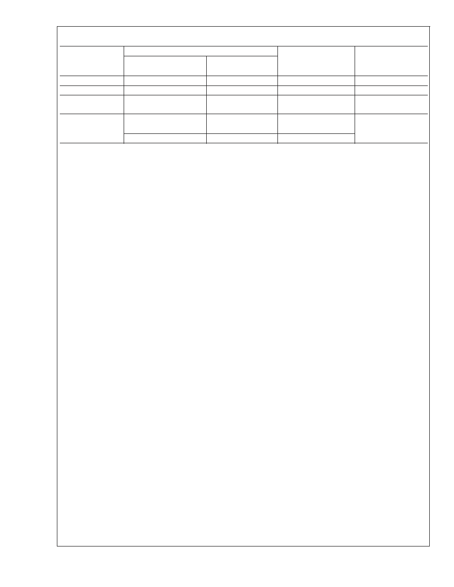
LM6172 Driving Capacitive Load
01258150
01258144
Connection Diagram
8-Pin DIP/SO
01258101
Top View
VIP
TM
is a trademark of National Semiconductor Corporation.
PAL
Æ
is a registered trademark of and used under license from Advanced Micro Devices, Inc.
April 2003
LM6172
Dual
High
Speed,
Low
Power
,
Low
Distortion,
V
oltage
Feedback
Amplifiers
© 2003 National Semiconductor Corporation
DS012581
www.national.com
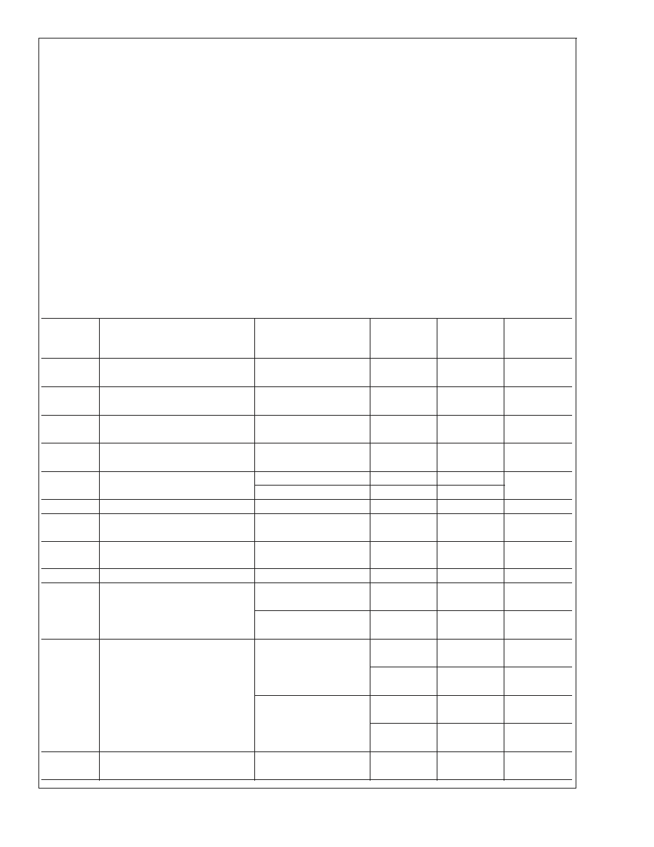
Ordering Information
Package
Temperature Range
Transport Media
NSC Drawing
Industrial
Military
-40∞C to +85∞C
-55∞C to +125∞C
8-Pin DIP
LM6172IN
Rails
N08E
8-Pin CDIP
LM6172AMJ-QML
5962-95604
Rails
J08A
16-Pin Ceramic
SOIC
LM6172AMWG-QML
5962-95604
Trays
WG16A
8-Pin
LM6172IM
Rails
M08A
Small Outline
LM6172IMX
Tape and Reel
LM6172
www.national.com
2
Absolute Maximum Ratings
(Note 1)
If Military/Aerospace specified devices are required,
please contact the National Semiconductor Sales Office/
Distributors for availability and specifications.
ESD Tolerance (Note 2)
Human Body Model
3kV
Machine Model
300V
Supply Voltage (V
+
- V
-
)
36V
Differential Input Voltage
±
10V
Common Mode Voltage Range
V
+
+0.3V to V
-
-0.3V
Input Current
±
10mA
Output Short Circuit to Ground
(Note 3)
Continuous
Storage Temp. Range
-65∞C to +150∞C
Maximum Junction Temperature
(Note 4)
150∞C
Soldering Information
Infrared or Convection Reflow
(20 sec.)
235∞C
Wave Soldering Lead Temp
(10 sec.)
260∞C
Operating Ratings
(Note 1)
Supply Voltage
5.5V
V
S
36V
Operating Temperature Range
LM6172I
-40∞C to +85∞C
Thermal Resistance (
JA
)
N Package, 8-Pin Molded DIP
95∞C/W
M Package, 8-Pin Surface Mount
160∞C/W
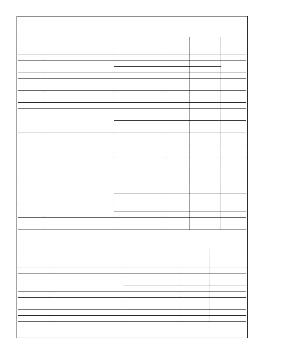
±
15V DC Electrical Characteristics
Unless otherwise specified, all limits guaranteed for T
J
= 25∞C,V
+
= +15V, V
-
= -15V, V
CM
= 0V, and R
L
= 1k
. Boldface
limits apply at the temperature extremes
Symbol
Parameter
Conditions
Typ
(Note 5)
LM6172I
Limit
(Note 6)
Units
V
OS
Input Offset Voltage
0.4
3
mV
4
max
TC V
OS
Input Offset Voltage
6
µV/∞C
Average Drift
I
B
Input Bias Current
1.2
3
µA
4
max
I
OS
Input Offset Current
0.02
2
µA
3
max
R
IN
Input Resistance
Common Mode
40
M
Differential Mode
4.9
R
O
Open Loop Output Resistance
14
CMRR
Common Mode Rejection Ratio
V
CM
=
±
10V
110
70
dB
65
min
PSRR
Power Supply Rejection Ratio
V
S
=
±
15V to
±
5V
95
75
70
dB
min
V
CM
Input Common Mode Voltage Range CMRR
60dB
±
13.5
V
A
V
Large Signal Voltage
R
L
= 1k
86
80
dB
Gain (Note 7)
75
min
R
L
= 100
78
65
dB
60
min
V
O
Output Swing
R
L
= 1k
13.2
12.5
V
12
min
-13.1
-12.5
V
-12
max
R
L
= 100
9
6
V
5
min
-8.5
-6
V
-5
max
Continuous Output Current
Sourcing, R
L
= 100
90
60
mA
(Open Loop) (Note 8)
50
min
LM6172
www.national.com
3
±
15V DC Electrical Characteristics
(Continued)
Unless otherwise specified, all limits guaranteed for T
J
= 25∞C,V
+
= +15V, V
-
= -15V, V
CM
= 0V, and R
L
= 1k
. Boldface
limits apply at the temperature extremes
Symbol
Parameter
Conditions
Typ
(Note 5)
LM6172I
Limit
(Note 6)
Units
Sinking, R
L
= 100
-85
-60
mA
-50
max
I
SC
Output Short Circuit
Sourcing
107
mA
Current
Sinking
-105
mA
I
S
Supply Current
Both Amplifiers
4.6
8
mA
9
max
±
15V AC Electrical Characteristics
Unless otherwise specified, T
J
= 25∞C, V
+
= +15V, V
-
= -15V, V
CM
= 0V, and R
L
= 1k
LM6172I
Symbol
Parameter
Conditions
Typ
Units
(Note 5)
SR
Slew Rate
A
V
= +2, V
IN
= 13 V
PP
3000
V/µs
A
V
= +2, V
IN
= 10 V
PP
2500
V/µs
Unity-Gain Bandwidth
100
MHz
-3 dB Frequency
A
V
= +1
160
MHz
A
V
= +2
62
MHz
Bandwidth Matching between Channels
2
MHz
m
Phase Margin
40
Deg
t
s
Settling Time (0.1%)
A
V
= -1, V
OUT
=
±
5V,
65
ns
R
L
= 500
A
D
Differential Gain (Note 9)
0.28
%
D
Differential Phase (Note 9)
0.6
Deg
e
n
Input-Referred
f = 1kHz
12
Voltage Noise
i
n
Input-Referred
f = 1kHz
1
Current Noise
Second Harmonic
f = 10kHz
-110
dB
Distortion (Note 10)
f = 5MHz
-50
dB
Third Harmonic
f = 10kHz
-105
dB
Distortion (Note 10)
f = 5MHz
-50
dB
±
5V DC Electrical Characteristics
Unless otherwise specified, all limits guaranteed for T
J
= 25∞C, V
+
= +5V, V
-
= -5V, V
CM
= 0V, and R
L
= 1 k
. Boldface lim-
its apply at the temperature extremes
Symbol
Parameter
Conditions
Typ
(Note 5)
LM6172I
Limit
(Note 6)
Units
V
OS
Input Offset Voltage
0.1
3
mV
4
max
TC V
OS
Input Offset Voltage
4
µV/∞C
Average Drift
I
B
Input Bias Current
1.4
2.5
µA
3.5
max
I
OS
Input Offset Current
0.02
1.5
µA
LM6172
www.national.com
4
±
5V DC Electrical Characteristics
(Continued)
Unless otherwise specified, all limits guaranteed for T
J
= 25∞C, V
+
= +5V, V
-
= -5V, V
CM
= 0V, and R
L
= 1 k
. Boldface lim-
its apply at the temperature extremes
Symbol
Parameter
Conditions
Typ
(Note 5)
LM6172I
Limit
(Note 6)
Units
2.2
max
R
IN
Input Resistance
Common Mode
40
M
Differential Mode
4.9
R
O
Output Resistance
14
CMRR
Common Mode Rejection Ratio
V
CM
=
±
2.5V
105
70
dB
65
min
PSRR
Power Supply Rejection Ratio
V
S
=
±
15V to
±
5V
95
75
dB
70
min
V
CM
Input Common Mode Voltage Range
CMRR
60dB
±
3.7
V
A
V
Large Signal Voltage
R
L
= 1k
82
70
dB
Gain (Note 7)
65
min
R
L
= 100
78
65
dB
60
min
V
O
Output Swing
R
L
= 1k
3.4
3.1
V
3
min
-3.3
-3.1
V
-3
max
R
L
= 100
2.9
2.5
V
2.4
min
-2.7
-2.4
V
-2.3
max
Continuous Output Current
Sourcing, R
L
= 100
29
25
mA
(Open Loop) (Note 8)
24
min
Sinking, R
L
= 100
-27
-24
mA
-23
max
I
SC
Output Short Circuit
Sourcing
93
mA
Current
Sinking
-72
mA
I
S
Supply Current
Both Amplifiers
4.4
6
mA
7
max
±
5V AC Electrical Characteristics
Unless otherwise specified, T
J
= 25∞C, V
+
= +5V, V
-
= -5V, V
CM
= 0V, and R
L
= 1 k
.
LM61722
Typ
(Note 5)
Symbol
Parameter
Conditions
Units
SR
Slew Rate
A
V
= +2, V
IN
= 3.5 V
PP
750
V/µs
Unity-Gain Bandwidth
70
MHz
-3 dB Frequency
A
V
= +1
130
MHz
A
V
= +2
45
MHz
m
Phase Margin
57
Deg
t
s
Settling Time (0.1%)
A
V
= -1, V
OUT
=
±
1V,
72
ns
R
L
= 500
A
D
Differential Gain (Note 9)
0.4
%
D
Differential Phase (Note 9)
0.7
Deg
LM6172
www.national.com
5