54AC161
∑
54ACT161
Synchronous Presettable Binary Counter
General Description
The 'AC/'ACT161 are high-speed synchronous modulo-16
binary counters. They are synchronously presettable for ap-
plication in programmable dividers and have two types of
Count Enable inputs plus a Terminal Count output for versa-
tility in forming synchronous multistage counters. The 'AC/
'ACT161 has an asynchronous Master Reset input that over-
rides all other inputs and forces the outputs LOW.
Features
n
I
CC
reduced by 50%
n
Synchronous counting and loading
n
High-speed synchronous expansion
n
Typical count rate of 125 MHz
n
Outputs source/sink 24 mA
n
'ACT161 has TTL-compatible inputs
n
Standard Microcircuit Drawing (SMD)
-- 'AC161: 5962-89561
-- 'ACT161: 5962-91722
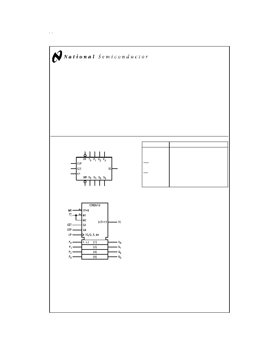
Logic Symbols
Pin Names
Description
CEP
Count Enable Parallel Input
CET
Count Enable Trickle Input
CP
Clock Pulse Input
MR
Asynchronous Master Reset Input
P
0
≠P
3
Parallel Data Inputs
PE
Parallel Enable Inputs
Q
0
≠Q
3
Flip-Flop Outputs
TC
Terminal Count Output
TRI-STATE
Æ
is a registered trademark of National Semiconductor Corporation.
FACT
TM
is a trademark of Fairchild Semiconductor Corporation.
DS100274-1
IEEE/IEC
DS100274-2
November 1998
54AC161
∑
54ACT161
Synchronous
Presettable
Binary
Counter
© 1998 National Semiconductor Corporation
DS100274
www.national.com

Connection Diagrams
Functional Description
The 'AC/'ACT161 count in modulo-16 binary sequence.
From state 15 (HHHH) they increment to state 0 (LLLL). The
clock inputs of all flip-flops are driven in parallel through a
clock buffer. Thus all changes of the Q outputs (except due
to Master Reset of the '161) occur as a result of, and syn-
chronous with, the LOW-to-HIGH transition of the CP input
signal. The circuits have four fundamental modes of opera-
tion, in order of precedence: asynchronous reset, parallel
load, count-up and hold. Five control inputs -- Master Reset,
Parallel Enable (PE), Count Enable Parallel (CEP) and
Count Enable Trickle (CET) -- determine the mode of opera-
tion, as shown in the Mode Select Table. A LOW signal on
MR overrides all other inputs and asynchronously forces all
outputs LOW. A LOW signal on PE overrides counting and
allows information on the Parallel Data (P
n
) inputs to be
loaded into the flip-flops on the next rising edge of CP. With
PE and MR HIGH, CEP and CET permit counting when both
are HIGH. Conversely, a LOW signal on either CEP or CET
inhibits counting.
The 'AC/'ACT161 use D-type edge-triggered flip-flops and
changing the PE, CEP and CET inputs when the CP is in ei-
ther state does not cause errors, provided that the recom-
mended setup and hold times, with respect to the rising edge
of CP, are observed.
The Terminal Count (TC) output is HIGH when CET is HIGH
and counter is in state 15. To implement synchronous multi-
stage counters, the TC outputs can be used with the CEP
and CET inputs in two different ways.
Figure 1 shows the connections for simple ripple carry, in
which the clock period must be longer than the CP to TC de-
lay of the first stage, plus the cumulative CET to TC delays of
the intermediate stages, plus the CET to CP setup time of
the last stage. This total delay plus setup time sets the upper
limit on clock frequency. For faster clock rates, the carry loo-
kahead connections shown in
Figure 2 are recommended. In
this scheme the ripple delay through the intermediate stages
commences with the same clock that causes the first stage
to tick over from max to min in the Up mode, or min to max
in the Down mode, to start its final cycle. Since this final
cycle requires 16 clocks to complete, there is plenty of time
for the ripple to progress through the intermediate stages.
The critical timing that limits the clock period is the CP to TC
delay of the first stage plus the CEP to CP setup time of the
last stage. The TC output is subject to decoding spikes due
to internal race conditions and is therefore not recom-
mended for use as a clock or asynchronous reset for
flip-flops, registers or counters.
Logic Equations: Count Enable = CEP
∑ CET ∑ PE
TC = Q
0
∑ Q
1
∑ Q
2
∑ Q
3
∑ CET
Mode Select Table
PE
CET
CEP
Action on the Rising
Clock Edge (
N
)
X
X
X
Reset (Clear)
L
X
X
Load (P
n
Q
n
)
H
H
H
Count (Increment)
H
L
X
No Change (Hold)
H
X
L
No Change (Hold)
H = HIGH Voltage Level
L = LOW Voltage Level
X = Immaterial
State Diagram
Pin Assignment
for DIP and Flatpak
DS100274-3
Pin Assignment
for LCC
DS100274-4
DS100274-5
www.national.com
2

State Diagram
(Continued)
DS100274-8
FIGURE 1. Multistage Counter with Ripple Carry
DS100274-9
FIGURE 2. Multistage Counter with Lookahead Carry
www.national.com
3
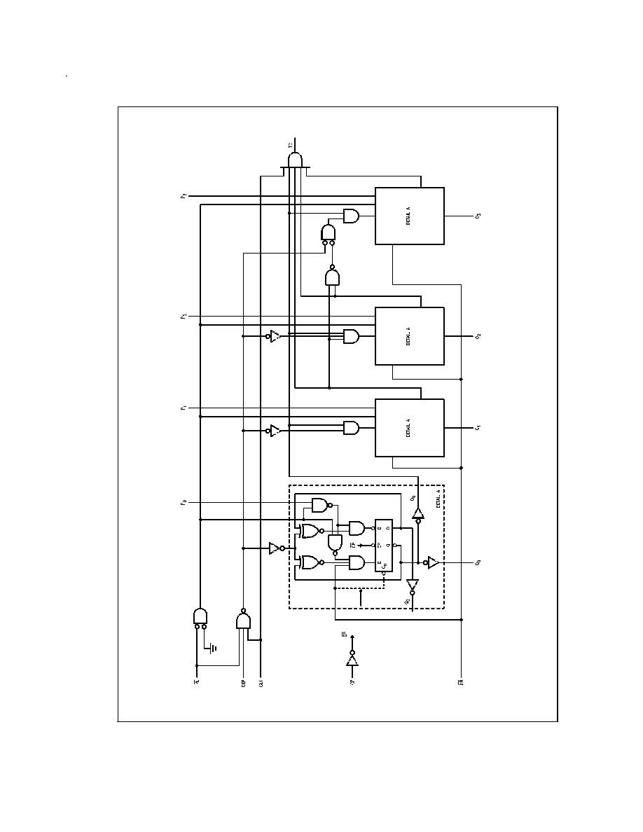
Block Diagram
DS100274-6
Please
note
that
this
diagram
is
provided
only
for
the
understanding
of
logic
operations
and
should
not
be
used
to
estimate
propagation
delays.
www.national.com
4

Absolute Maximum Ratings
(Note 1)
If Military/Aerospace specified devices are required,
please contact the National Semiconductor Sales Office/
Distributors for availability and specifications.
Supply Voltage (V
CC
)
-0.5V to +7.0V
DC Input Diode Current (I
IK
)
V
I
= -0.5V
-20 mA
V
I
= V
CC
+ 0.5V
+20 mA
DC Input Voltage (V
I
)
-0.5V to V
CC
+ 0.5V
DC Output Diode Current (I
OK
)
V
O
= -0.5V
-20 mA
V
O
= V
CC
+ 0.5V
+20 mA
DC Output Voltage (V
O
)
-0.5V to V
CC
+ 0.5V
DC Output Source
or Sink Current (I
O
)
±
50 mA
DC V
CC
or Ground Current
per Output Pin (I
CC
or I
GND
)
±
50 mA
Storage Temperature (T
STG
)
-65∞C to +150∞C
Junction Temperature (T
J
)
CDIP
175∞C
Recommended Operating
Conditions
Supply Voltage (V
CC
)
'AC
2.0V to 6.0V
'ACT
4.5V to 5.5V
Input Voltage (V
I
)
0V to V
CC
Output Voltage (V
O
)
0V to V
CC
Operating Temperature (T
A
)
54AC/ACT
-55∞C to +125∞C
Minimum Input Edge Rate (
V/
t)
'AC Devices
V
IN
from 30% to 70% of V
CC
V
CC
@
3.3V, 4.5V, 5.5V
125 mV/ns
Minimum Input Edge Rate (
V/
t)
'ACT Devices
V
IN
from 0.8V to 2.0V
V
CC
@
4.5V, 5.5V
125 mV/ns
Note 1: Absolute maximum ratings are those values beyond which damage
to the device may occur. The databook specifications should be met, without
exception, to ensure that the system design is reliable over its power supply,
temperature, and output/input loading variables. National does not recom-
mend operation of FACT
TM
circuits outside databook specifications.
DC Characteristics for 'AC Family Devices
54AC
Symbol
Parameter
V
CC
T
A
=
Units
Conditions
(V)
-55∞C to +125∞C
Guaranteed Limits
V
IH
Minimum High Level
3.0
2.1
V
OUT
= 0.1V
Input Voltage
4.5
3.15
V
or V
CC
- 0.1V
5.5
3.85
V
IL
Maximum Low Level
3.0
0.9
V
OUT
= 0.1V
Input Voltage
4.5
1.35
V
or V
CC
- 0.1V
5.5
1.65
V
OH
Minimum High Level
3.0
2.9
I
OUT
= -50 µA
Output Voltage
4.5
4.4
V
5.5
5.4
(Note 2)
V
IN
= V
IL
or V
IH
3.0
2.4
I
OH
= -12 mA
4.5
3.7
V
I
OH
= -24 mA
5.5
4.7
I
OH
= -24 mA
V
OL
Maximum Low Level
3.0
0.1
I
OUT
= 50 µA
Output Voltage
4.5
0.1
V
5.5
0.1
(Note 2)
V
IN
= V
IL
or V
IH
3.0
0.5
I
OL
= 12 mA
4.5
0.5
V
I
OL
= 24 mA
5.5
0.5
I
OL
= 24 mA
I
IN
Maximum Input
5.5
±
1.0
µA
V
I
= V
CC
, GND
Leakage Current
I
OLD
Minimum Dynamic
Output Current (Note 3)
5.5
50
mA
V
OLD
= 1.65V Max
I
OHD
5.5
-50
mA
V
OHD
= 3.85V Min
I
CC
Maximum Quiescent
5.5
160
µA
V
IN
= V
CC
www.national.com
5