TL F 6547
54153DM54153DM74153
Dual
4-Line
to
1-Line
Data
SelectorsMultiplexers
June 1989
54153 DM54153 DM74153 Dual 4-Line to 1-Line
Data Selectors Multiplexers
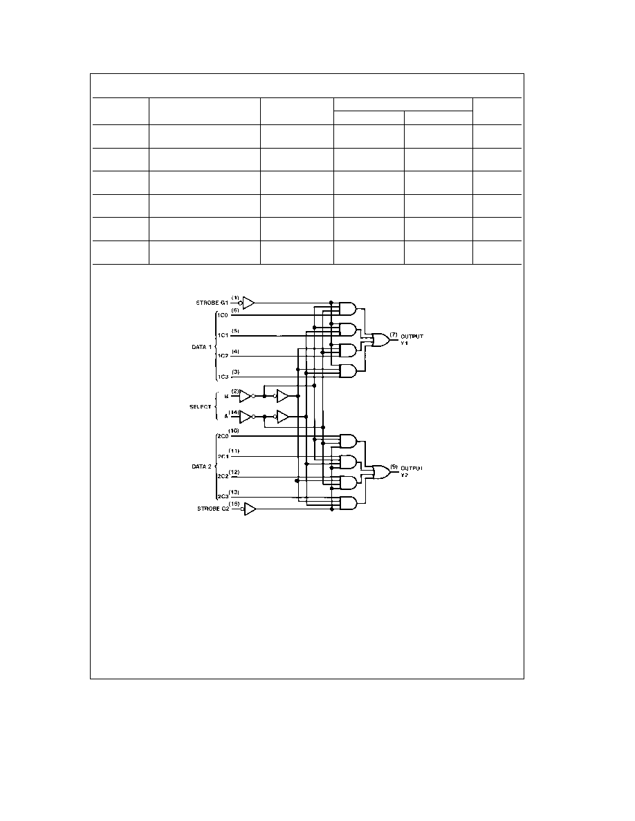
General Description
Each of these data selectors multiplexers contains invert-
ers and drivers to supply fully complementary on-chip bina-
ry decoding data selection to the AND-OR-invert gates
Separate strobe inputs are provided for each of the two
four-line sections
Features
Y
Permits multiplexing from N lines to 1 line
Y
Performs parallel-to-serial conversion
Y
Strobe (enable) line provided for cascading (N lines to
n lines)
Y
High fan-out low-impedance totem-pole outputs
Y
Typical average propagation delay times
From data 11 ns
From strobe 18 ns
From select 20 ns
Y
Typical power dissipation 170 mW
Y
Alternate Military Aerospace device (54153) is avail-
able Contact a National Semiconductor Sales Office
Distributor for specifications
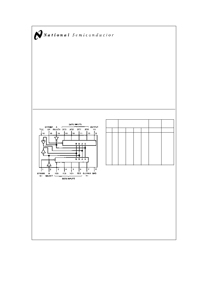
Connection Diagram
Dual-In-Line Package
TL F 6547 ≠ 1
Order Number 54153DMQB 54153FMQB DM54153J
DM54153W or DM74153N
See NS Package Number J16A N16E or W16A
Function Table
Select
Data Inputs
Strobe
Output
Inputs
B
A
C0
C1
C2
C3
G
Y
X
X
X
X
X
X
H
L
L
L
L
X
X
X
L
L
L
L
H
X
X
X
L
H
L
H
X
L
X
X
L
L
L
H
X
H
X
X
L
H
H
L
X
X
L
X
L
L
H
L
X
X
H
X
L
H
H
H
X
X
X
L
L
L
H
H
X
X
X
H
L
H
Select inputs A and B are common to both sections
H
e
High Level L
e
Low Level X
e
Don't Care
C1995 National Semiconductor Corporation
RRD-B30M105 Printed in U S A
Absolute Maximum Ratings
(Note)
If Military Aerospace specified devices are required
please contact the National Semiconductor Sales
Office Distributors for availability and specifications
Supply Voltage
7V
Input Voltage
5 5V
Operating Free Air Temperature Range
DM54 and 54
b
55 C to
a
125 C
DM74
0 C to
a
70 C
Storage Temperature Range
b
65 C to
a
150 C
Note
The ``Absolute Maximum Ratings'' are those values
beyond which the safety of the device cannot be guaran-
teed The device should not be operated at these limits The
parametric values defined in the ``Electrical Characteristics''
table are not guaranteed at the absolute maximum ratings
The ``Recommended Operating Conditions'' table will define
the conditions for actual device operation
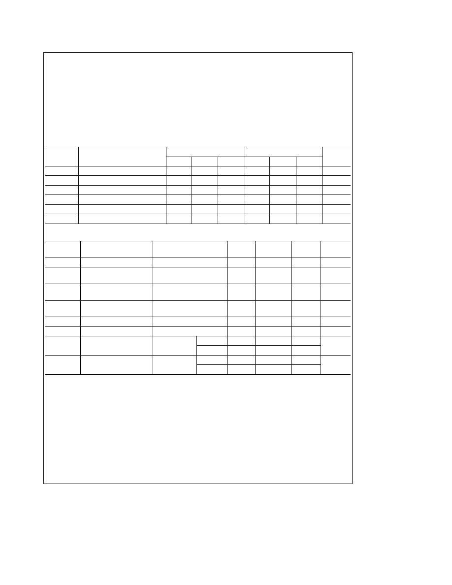
Recommended Operating Conditions
Symbol
Parameter
DM54153
DM74153
Units
Min
Nom
Max
Min
Nom
Max
V
CC
Supply Voltage
4 5
5
5 5
4 75
5
5 25
V
V
IH
High Level Input Voltage
2
2
V
V
IL
Low Level Input Voltage
0 8
0 8
V
I
OH
High Level Output Current
b
0 8
b
0 8
mA
I
OL
Low Level Output Current
16
16
mA
T
A
Free Air Operating Temperature
b
55
125
0
70
C
Electrical Characteristics
over recommended operating free air temperature range (unless otherwise noted)
Symbol
Parameter
Conditions
Min
Typ
Max
Units
(Note 1)
V
I
Input Clamp Voltage
V
CC
e
Min I
I
e b
12 mA
b
1 5
V
V
OH
High Level Output
V
CC
e
Min I
OH
e
Max
2 4
3 2
V
Voltage
V
IL
e
Max V
IH
e
Min
V
OL
Low Level Output
V
CC
e
Min I
OL
e
Max
0 2
0 4
V
Voltage
V
IH
e
Min V
IL
e
Max
I
I
Input Current
Max
V
CC
e
Max V
I
e
5 5V
1
mA
Input Voltage
I
IH
High Level Input Current
V
CC
e
Max V
I
e
2 4V
40
m
A
I
IL
Low Level Input Current
V
CC
e
Max V
I
e
0 4V
b
1 6
mA
I
OS
Short Circuit
V
CC
e
Max
DM54
b
20
b
55
mA
Output Current
(Note 2)
DM74
b
18
b
57
I
CC
Supply Current
V
CC
e
Max
DM54
34
52
mA
(Note 3)
DM74
34
60
Note 1
All typicals are at V
CC
e
5V T
A
e
25 C
Note 2
Not more than one output should be shorted at a time
Note 3
I
CC
is measured with the outputs open and all inputs grounded
2
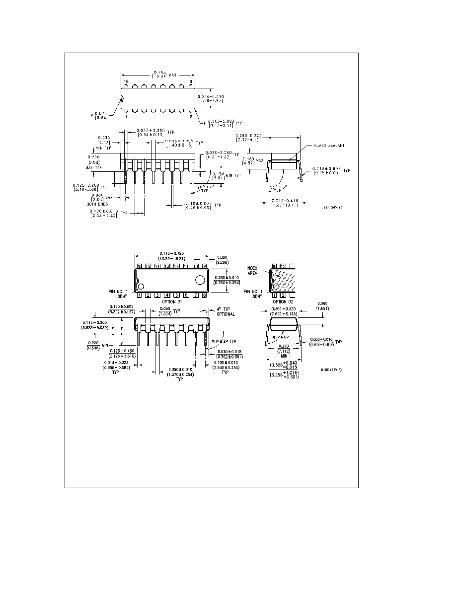
Physical Dimensions
inches (millimeters)
16-Lead Ceramic Dual-In-Line Package (J)
Order Number 54153DMQB or DM54153J
NS Package Number J16A
16-Lead Molded Dual-In-Line Package (N)
Order Number DM74153N
NS Package Number N16E
5