TL F 6561
DM74184DM74185A
BCD-to-Binary
and
Binary-to-BCD
Converters
June 1989
DM74184 DM74185A
BCD-to-Binary and Binary-to-BCD Converters
General Description
These monolithic converters are derived from the 256-bit
read only memories DM5488 and DM7488 Emitter con-
nections are made to provide direct read-out of converted
codes at outputs Y8 through Y1 as shown in the function
tables These converters demonstrate the versatility of a
read only memory in that an unlimited number of reference
tables or conversion tables may be built into a system Both
of these converters comprehend that the least significant
bits (LSB) of the binary and BCD codes are logically equal
and in each case the LSB bypasses the converter as illus-
trated in the typical applications This means that a 6-bit
converter is produced in each case Both devices are cas-
cadable to N bits
An overriding enable input is provided on each converter
which when taken high inhibits the function causing all out-
puts to go high For this reason and to minimize power
consumption unused outputs Y7 and Y8 of the 185A and all
``don't care'' conditions of the 184 are programmed high
The outputs are of the open-collector type
DM74184 BCD-TO-BINARY CONVERTERS
The 6-bit BCD-to-binary function of the DM74184 is analo-
gous to the algorithm
a Shift BCD number right one bit and examine each dec-
ade Subtract three from each 4-bit decade containing a
binary value greater than seven
b Shift right examine and correct after each shift until the
least significant decade contains a number smaller than
eight and all other converted decades contain zeros
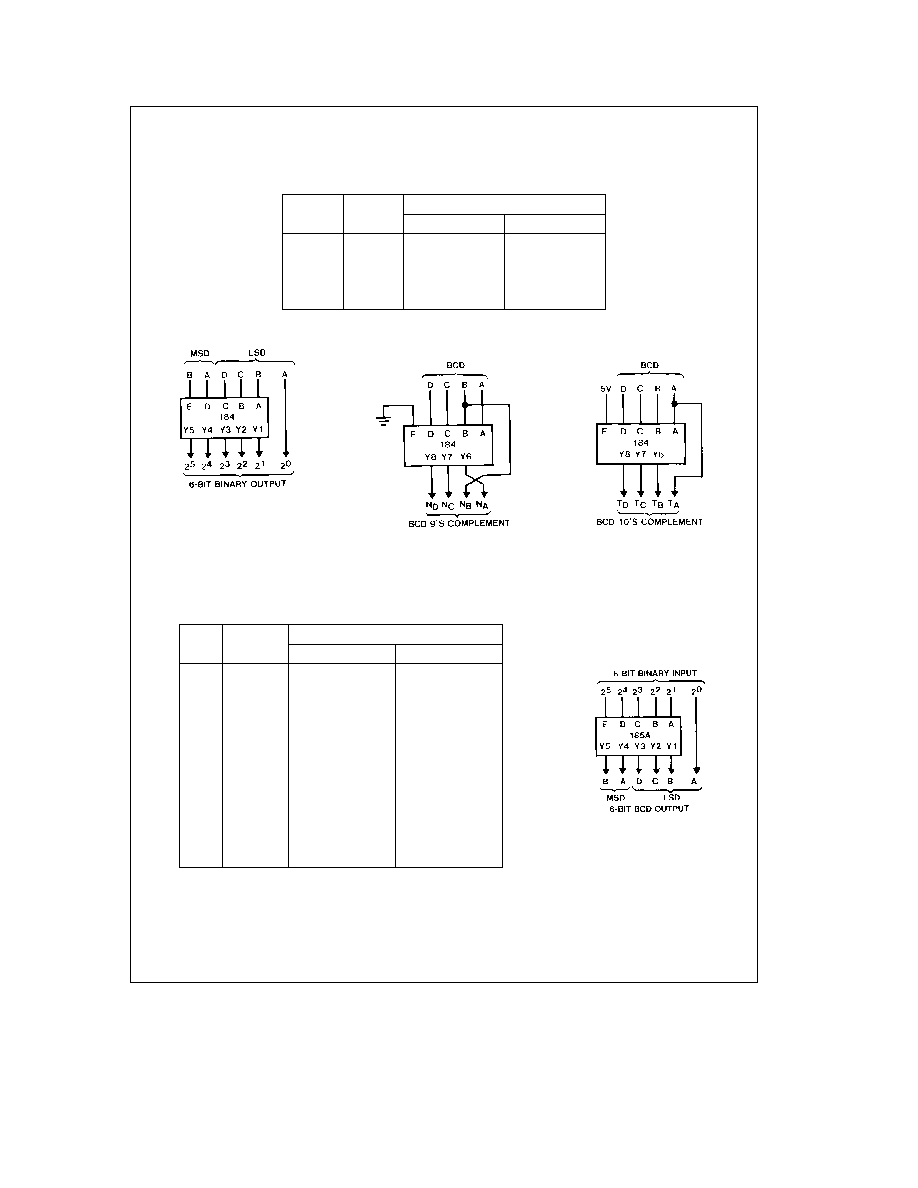
In addition to BCD-to-binary conversion the DM74184 is
programmed to generate BCD 9's complement or BCD 10's
complement Again in each case one bit of the comple-
ment code is logically equal to one of the BCD bits there-
fore these complements can be produced on three lines
As outputs Y6 Y7 and Y8 are not required in the BCD-to-bi-
nary conversion they are utilized to provide these comple-
ment codes as specified in the function table when the de-
vices are connected as shown
DM74185A BINARY-TO-BCD CONVERTERS
The function performed by these 6-bit binary-to-BCD con-
verters is analogous to the algorithm
a Examine the three most significant bits If the sum is
greater than four add three and shift left one bit
b Examine each BCD decade If the sum is greater than
four add three and shift left one bit
c Repeat step b until the least-significant binary bit is in the
least-significant BCD location
(Continued)
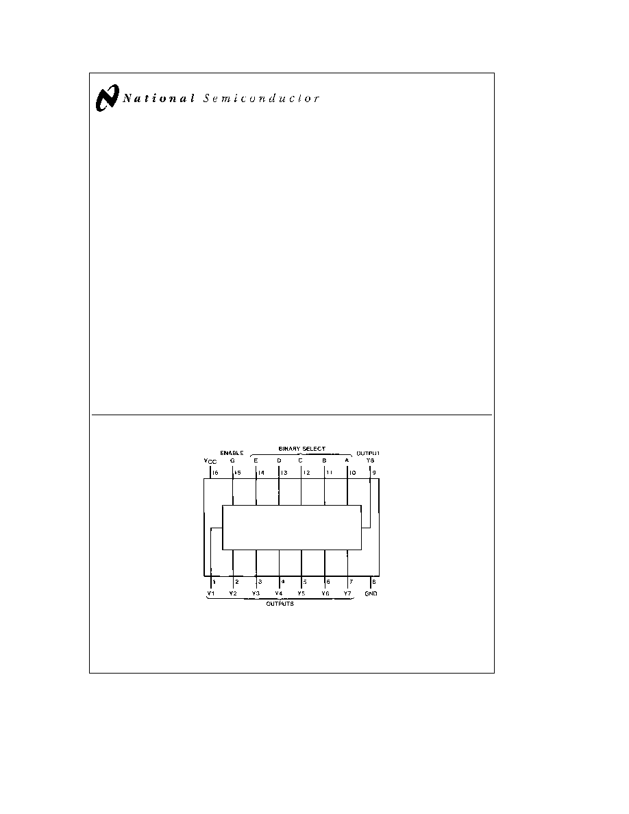
Connection Diagram
TL F 6561 ≠ 1
Order Number DM74184N or DM74185AN
See NS Package Number N16E
C1995 National Semiconductor Corporation
RRD-B30M105 Printed in U S A

Absolute Maximum Ratings
(Note)
If Military Aerospace specified devices are required
please contact the National Semiconductor Sales
Office Distributors for availability and specifications
Supply Voltage
7V
Input Voltage
5 5V
Output Voltage
7V
Operating Free Air Temperature
Range
0 C to
a
70 C
Storage Temperature Range
b
65 C to
a
150 C
Note
The ``Absolute Maximum Ratings'' are those values
beyond which the safety of the device cannot be guaran-
teed The device should not be operated at these limits The
parametric values defined in the ``Electrical Characteristics''
table are not guaranteed at the absolute maximum ratings
The ``Recommended Operating Conditions'' table will define
the conditions for actual device operation
Recommended Operating Conditions
Symbol
Parameter
Min
Nom
Max
Units
V
CC
Supply Voltage
4 75
5
5 25
V
V
IH
High Level Input Voltage
2
V
V
IL
Low Level Input Voltage
0 8
V
V
OH
High Level Output Voltage
5 5
V
I
OL
Low Level Output Current
12
mA
T
A
Free Air Operating Temperature
0
70
C
'184 and '185A Electrical Characteristics
over recommended operating free air temperature range (unless otherwise noted)
Symbol
Parameter
Conditions
Min
Typ
Max
Units
(Note 1)
V
I
Input Clamp Voltage
V
CC
e
Min I
I
e b
12 mA
b
1 5
V
I
CEX
High Level Output
V
CC
e
Min V
O
e
5 5V
100
m
A
Current
V
IL
e
Max V
IH
e
Min
V
OL
Low Level Output
V
CC
e
Min I
OL
e
Max
0 4
V
Voltage
V
IH
e
Min V
IL
e
Max
I
I
Input Current
Max
V
CC
e
Max V
I
e
5 5V
1
mA
Input Voltage
I
IH
High Level Input Current
V
CC
e
Max V
I
e
2 4V
25
m
A
I
IL
Low Level Input Current
V
CC
e
Max V
I
e
0 4V
b
1
mA
I
CCH
Supply Current with
V
CC
e
Max
65
95
mA
Outputs High
I
CCL
Supply Current with
V
CC
e
Max
80
99
mA
Outputs Low
'184 and '185A Switching Characteristics
at V
CC
e
5V and T
A
e
25 C (See Section 1 for Test Waveforms and Output Load)
From (Input)
R
L1
e
400X R
L2
e
600X
Symbol
Parameter
To (Output)
C
L
e
15 pF (See Test Circuit)
Units
Min
Max
t
PLH
Propagation Delay Time
Enable G
35
ns
Low to High Level Output
to Output
t
PHL
Propagation Delay Time
Enable G
35
ns
High to Low Level Output
to Output
t
PLH
Propagation Delay Time
Binary Select
35
ns
Low to High Level Output
to Output
t
PHL
Propagation Delay Time
Binary Select
35
ns
High to Low Level Output
to Output
Note 1
All typicals are at V
CC
e
5V T
A
e
25 C
2

General Description
(Continued)
DM74184 BCD-to-Binary
TABLE I Package Count and Delay Times
for BCD-to-Binary Conversion
Input
Packages
Total Delay Times (ns)
(Decades)
Required
Typ
Max
2
2
56
80
3
6
140
200
4
12
196
280
5
19
280
400
6
28
364
520
6-Bit Converter
TL F 6561 ≠ 2
BCD 9's
Complement Converter
TL F 6561 ≠ 3
BCD's 10's
Complement Converter
TL F 6561 ≠ 4
DM74185A Binary-to-BCD
TABLE II Package Count and Delay Times
for Binary-to-BCD Conversion
Input
Packages
Total Delay Times (ns)
(Bits)
Required
Typ
Max
4 to 6
1
25
40
7 or 8
3
50
80
9
4
75
120
10
6
100
160
11
7
125
200
12
8
125
200
13
10
150
240
14
12
175
280
15
14
175
280
16
16
200
320
17
19
225
360
18
21
225
360
19
24
250
400
20
27
275
440
6-Bit Converter
TL F 6561 ≠ 5
3

Function Tables
(Continued)
BCD-to-Binary Converter
BCD
Inputs
Outputs
Words
(See Note A)
(See Note B)
E D C B A G Y5 Y4 Y3 Y2 Y1
0
1
L
L
L
L
L
L
L
L
L
L
L
2
3
L
L
L
L H L
L
L
L
L
H
4
5
L
L
L H L
L
L
L
L
H
L
6
7
L
L
L H H L
L
L
L
H
H
8
9
L
L H L
L
L
L
L
H
L
L
10
11
L H L
L
L
L
L
L
H
L
H
12
13
L H L
L H L
L
L
H
H
L
14
15
L H L H L
L
L
L
H
H
H
16
17
L H L H H L
L
H
L
L
L
18
19
L H H L
L
L
L
H
L
L
H
20
21
H L
L
L
L
L
L
H
L
H
L
22
23
H L
L
L H L
L
H
L
H
H
24
25
H L
L H L
L
L
H
H
L
L
26
27
H L
L H H L
L
H
H
L
H
28
29
H L H L
L
L
L
H
H
H
L
30
31
H H L
L
L
L
L
H
H
H
H
32
33
H H L
L H L
H
L
L
L
L
34
35
H H L H L
L
H
L
L
L
H
36
37
H H L H H L
H
L
L
H
L
38
39
H H H L
L
L
H
L
L
H
H
Any
X X X X X H
H
H
H
H
H
BCD 9's or BCD 10's Complement Converter
BCD
Inputs
Outputs
Word
(See Note C)
(See Note D)
E
D
C
B
A
G
Y8
Y7
Y6
0
L
L
L
L
L
L
H
L
H
1
L
L
L
L
H
L
H
L
L
2
L
L
L
H
L
L
L
H
H
3
L
L
L
H
H
L
L
H
L
4
L
L
H
L
L
L
L
H
H
5
L
L
H
L
H
L
L
H
L
6
L
L
H
H
L
L
L
L
H
7
L
L
H
H
H
L
L
L
L
8
L
H
L
L
L
L
L
L
H
9
L
H
L
L
H
L
L
L
L
0
H
L
L
L
L
L
L
L
L
1
H
L
L
L
H
L
H
L
L
2
H
L
L
H
L
L
H
L
L
3
H
L
L
H
H
L
L
H
H
4
H
L
H
L
L
L
L
H
H
5
H
L
H
L
H
L
L
H
L
6
H
L
H
H
L
L
L
H
L
7
H
L
H
H
H
L
L
L
H
8
H
H
L
L
L
L
L
L
H
9
H
H
L
L
H
L
L
L
L
Any
X
X
X
X
X
H
H
H
H
H
e
High Level L
e
Low Level X
e
Don't Care
Note A
Input Conditions other than those shown produce highs at outputs Y1 through Y5
Note B
Output Y6 Y7 and Y8 are not used for BCD-to-Binary conversion
Note C
Input conditions other than those shown produce highs at outputs Y6 Y7 and Y8
Note D
Outputs Y1 through Y5 are not used for BCD 9's or BCD 10's complement conversion
When these devices are used as complement converters input E is used as a mode control With this input low the BCD 9's complement is generated when it is
high the BCD 10's complement is generated
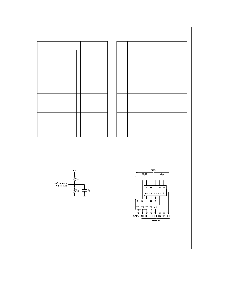
Test Circuit
TL F 6561 ≠ 6
C
L
includes probe and jig capacitance
Typical Applications
TL F 6561 ≠ 7
FIGURE 1 BCD-to-Binary Converter
for Two BCD Decades
MSD
Most significant decade
LSD
Least significant decade
Each rectangle represents a DM74184
5
