 | –≠–ª–µ–∫—Ç—Ä–æ–Ω–Ω—ã–π –∫–æ–º–ø–æ–Ω–µ–Ω—Ç: 7446A | –°–∫–∞—á–∞—Ç—å:  PDF PDF  ZIP ZIP |
TL F 6518
DM7446A
DM5447ADM7447A
BCD
to
7-Segment
DecodersDrivers
June 1989
DM7446A DM5447A DM7447A
BCD to 7-Segment Decoders Drivers
General Description
The 46A and 47A feature active-low outputs designed for
driving common-anode LEDs or incandescent indicators di-
rectly All of the circuits have full ripple-blanking input out-
put controls and a lamp test input Segment identification
and resultant displays are shown on a following page Dis-
play patterns for BCD input counts above nine are unique
symbols to authenticate input conditions
All of the circuits incorporate automatic leading and or trail-
ing-edge zero-blanking control (RBI and RBO) Lamp test
(LT) of these devices may be performed at any time when
the BI RBO node is at a high logic level All types contain
an overriding blanking input (BI) which can be used to con-
trol the lamp intensity (by pulsing) or to inhibit the outputs
Features
Y
All circuit types feature lamp intensity modulation
capability
Y
Open-collector outputs drive indicators directly
Y
Lamp-test provision
Y
Leading trailing zero suppression
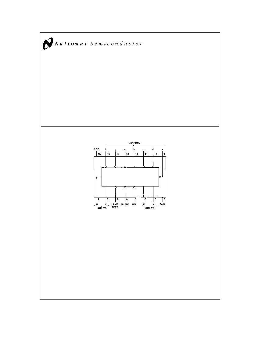
Connection Diagram
Dual-In-Line Package
TL F 6518 ≠ 1
Order Number DM5447AJ DM7446AN or DM7447AN
See NS Package Number J16A or N16E
C1995 National Semiconductor Corporation
RRD-B30M105 Printed in U S A
Absolute Maximum Ratings
(Note)
If Military Aerospace specified devices are required
please contact the National Semiconductor Sales
Office Distributors for availability and specifications
Supply Voltage
7V
Input Voltage
5 5V
Operating Free Air Temperature Range
DM54
b
55 C to
a
125 C
DM74
0 C to
a
70 C
Storage Temperature Range
b
65 C to
a
150 C
Note
The ``Absolute Maximum Ratings'' are those values
beyond which the safety of the device cannot be guaran-
teed The device should not be operated at these limits The
parametric values defined in the ``Electrical Characteristics''
table are not guaranteed at the absolute maximum ratings
The ``Recommended Operating Conditions'' table will define
the conditions for actual device operation
Recommended Operating Conditions
Symbol
Parameter
DM7446A
Units
Min
Nom
Max
V
CC
Supply Voltage
4 75
5
5 25
V
V
IH
High Level Input Voltage
2
V
V
IL
Low Level Input Voltage
0 8
V
V
OH
High Level Output Voltage (a thru g)
30
V
I
OH
High Level Output Current (BI RBO)
b
0 2
m
A
I
OL
Low Level Output Current (a thru g)
40
mA
I
OL
Low Level Output Current (BI RBO)
8
mA
T
A
Free Air Operating Temperature
0
70
C
'46A Electrical Characteristics
over recommended operating free air temperature range (unless otherwise noted)
Symbol
Parameter
Conditions
Min
Typ
Max
Units
(Note 1)
V
I
Input Clamp Voltage
V
CC
e
Min I
I
e b
12 mA
b
1 5
V
V
OH
High Level Output
V
CC
e
Min
2 4
3 7
V
Voltage (BI RBO)
I
OH
e
Max
I
CEX
High Level Output
V
CC
e
Max V
O
e
30V
250
m
A
Current (a thru g)
V
IL
e
Max V
IH
e
Min
V
OL
Low Level Output
V
CC
e
Min I
OL
e
Max
0 3
0 4
V
Voltage
V
IH
e
Min V
IL
e
Max
I
I
Input Current
Max
V
CC
e
Max V
I
e
5 5V
1
mA
Input Voltage
(Except BI RBO)
I
IH
High Level Input
V
CC
e
Max V
I
e
2 4V
40
m
A
Current
(Except BI RBO)
I
IL
Low Level Input
V
CC
e
Max
BI RBO
b
4
mA
Current
V
I
e
0 4V
Others
b
1 6
I
OS
Short Circuit
V
CC
e
Max (BI RBO)
b
4
mA
Output Current
I
CC
Supply Current
V
CC
e
Max
60
103
mA
(Note 2)
Note 1
All typicals are at V
CC
e
5V T
A
e
25 C
Note 2
I
CC
is measured with all outputs open and all inputs at 4 5V
2
'46A Switching Characteristics
at V
CC
e
5V and T
A
e
25 C (See Section 1 for Test Waveforms and Output Load)
Symbol
Parameter
Conditions
Min
Max
Units
t
PLH
Propagation Delay Time
C
L
e
15 pF
100
ns
Low to High Level Output
R
L
e
120X
t
PHL
Propagation Delay Time
100
ns
High to Low Level Output
Recommended Operating Conditions
Symbol
Parameter
DM5447A
DM7447A
Units
Min
Nom
Max
Min
Nom
Max
V
CC
Supply Voltage
4 5
5
5 5
4 75
5
5 25
V
V
IH
High Level Input Voltage
2
2
V
V
IL
Low Level Input Voltage
0 8
0 8
V
V
OH
High Level Output
15
15
V
Voltage (a thru g)
I
OH
High Level Output
b
0 2
b
0 2
m
A
Current (BI RBO)
I
OL
Low Level Output
40
40
mA
Current (a thru g)
I
OL
Low Level Output
8
8
mA
Current (BI RBO)
T
A
Free Air Operating Temperature
b
55
125
0
70
C
'47A Electrical Characteristics
over recommended operating free air temperature range (unless otherwise noted)
Symbol
Parameter
Conditions
Min
Typ
Max
Units
(Note 1)
V
I
Input Clamp Voltage
V
CC
e
Min I
I
e b
12 mA
b
1 5
V
V
OH
High Level Output
V
CC
e
Min
2 4
3 7
V
Voltage (BI RBO)
I
OH
e
Max
I
CEX
High Level Output
V
CC
e
Max V
O
e
15V
250
m
A
Current (a thru g)
V
IL
e
Max V
IH
e
Min
V
OL
Low Level Output
V
CC
e
Min I
OL
e
Max
0 3
0 4
V
Voltage
V
IH
e
Min V
IL
e
Max
I
I
Input Current
Max
V
CC
e
Max V
I
e
5 5V
1
mA
Input Voltage
I
IH
High Level Input Current
V
CC
e
Max V
I
e
2 4V
40
m
A
I
IL
Low Level Input
V
CC
e
Max
BI RBO
b
4
mA
Current
V
I
e
0 4V
Others
b
1 6
I
OS
Short Circuit
V
CC
e
Max (BI RBO)
b
4
mA
Output Current
I
CC
Supply Current
V
CC
e
Max
DM54
60
85
mA
(Note 2)
DM74
60
103
Note 1
All typicals are at V
CC
e
5V T
A
e
25 C
Note 2
I
CC
is measured with all outputs open and all inputs at 4 5V
3
'47A Switching Characteristics
at V
CC
e
5V and T
A
e
25 C (See Section 1 for Test Waveforms and Output Load)
Symbol
Parameter
Conditions
Min
Max
Units
t
PLH
Propagation Delay Time
C
L
e
15 pF
100
ns
Low to High Level Output
R
L
e
120X
t
PHL
Propagation Delay Time
100
ns
High to Low Level Output
Function Table
46A 47A
Decimal or
Inputs
BI RBO
Outputs
Note
Function
LT
RBI
D
C
B
A
(Note 1)
a
b
c
d
e
f
g
0
H
H
L
L
L
L
H
L
L
L
L
L
L
H
1
H
X
L
L
L
H
H
H
L
L
H
H
H
H
2
H
X
L
L
H
L
H
L
L
H
L
L
H
L
3
H
X
L
L
H
H
H
L
L
L
L
H
H
L
4
H
X
L
H
L
L
H
H
L
L
H
H
L
L
5
H
X
L
H
L
H
H
L
H
L
L
H
L
L
6
H
X
L
H
H
L
H
H
H
L
L
L
L
L
7
H
X
L
H
H
H
H
L
L
L
H
H
H
H
(2)
8
H
X
H
L
L
L
H
L
L
L
L
L
L
L
9
H
X
H
L
L
H
H
L
L
L
H
H
L
L
10
H
X
H
L
H
L
H
H
H
H
L
L
H
L
11
H
X
H
L
H
H
H
H
H
L
L
H
H
L
12
H
X
H
H
L
L
H
H
L
H
H
H
L
L
13
H
X
H
H
L
H
H
L
H
H
L
H
L
L
14
H
X
H
H
H
L
H
H
H
H
L
L
L
L
15
H
X
H
H
H
H
H
H
H
H
H
H
H
H
BI
X
X
X
X
X
X
L
H
H
H
H
H
H
H
(3)
RBI
H
L
L
L
L
L
L
H
H
H
H
H
H
H
(4)
LT
L
X
X
X
X
X
H
L
L
L
L
L
L
L
(5)
Note 1
BI RBO is a wire-AND logic serving as blanking input (BI) and or ripple-blanking output (RBO)
Note 2
The blanking input (BI) must be open or held at a high logic level when output functions 0 through 15 are desired The ripple-blanking input (RBI) must
be open or high if blanking of a decimal zero is not desired
Note 3
When a low logic level is applied directly to the blanking input (BI) all segment outputs are high regardless of the level of any other input
Note 4
When ripple-blanking input (RBI) and inputs A B C and D are at a low level with the lamp test input high all segment outputs go H and the ripple-
blanking output (RBO) goes to a low level (response condition)
Note 5
When the blanking input ripple-blanking output (BI RBO) is open or held high and a low is applied to the lamp-test input all segment outputs are L
H
e
High level L
e
Low level X
e
Don't Care
4
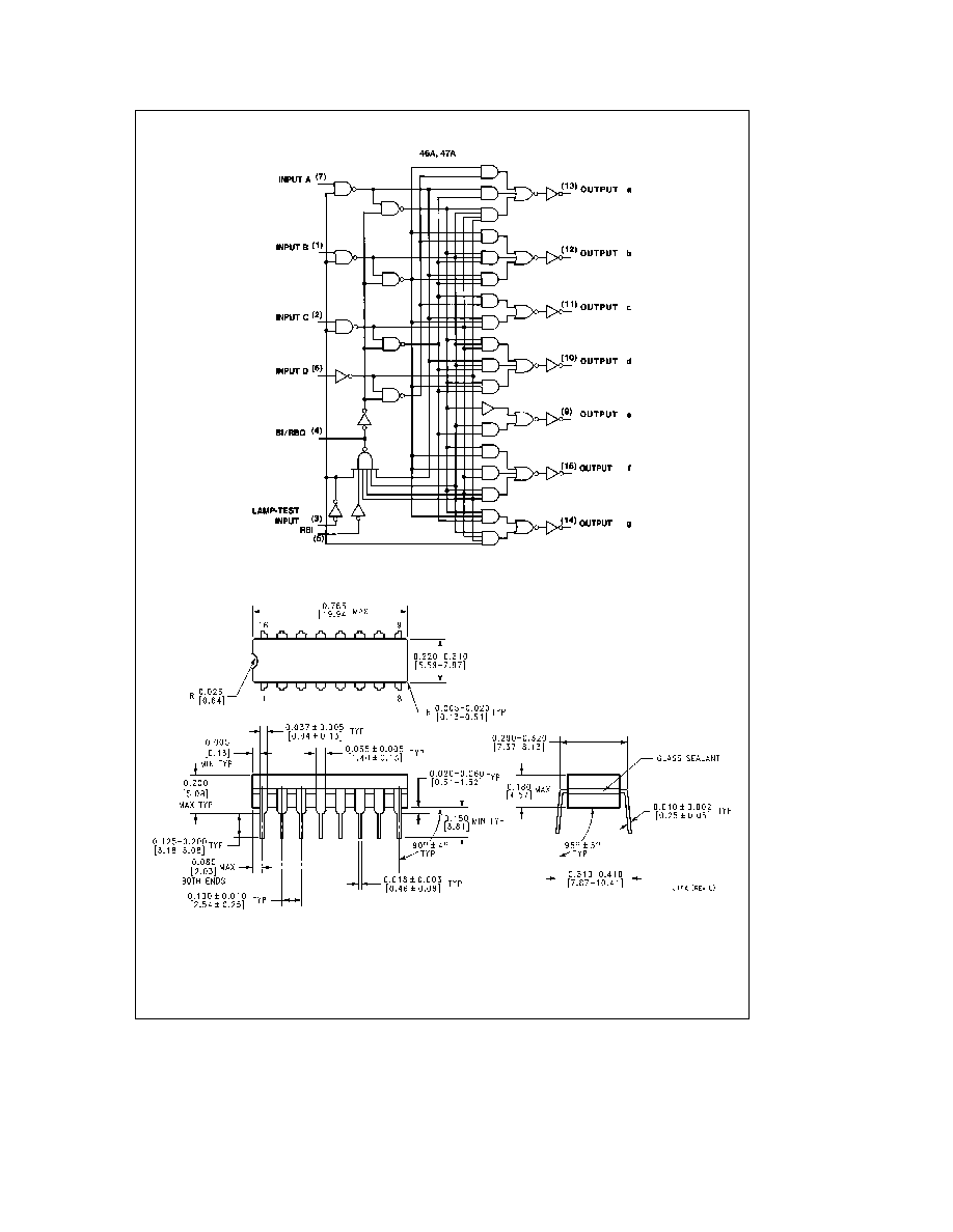
Logic Diagram
TL F 6518 ≠ 2
Physical Dimensions
inches (millimeters)
16-Lead Ceramic Dual-In-Line Package (J)
Order Number DM5447AJ
NS Package Number J16A
5