TL F 6379
54LS85DM54LS85DM74LS85
4-Bit
Magnitude
Comparators
June 1989
54LS85 DM54LS85 DM74LS85
4-Bit Magnitude Comparators
General Description
These 4-bit magnitude comparators perform comparison of
straight binary or BCD codes Three fully-decoded decisions
about two 4-bit words (A B) are made and are externally
available at three outputs These devices are fully expand-
able to any number of bits without external gates Words of
greater length may be compared by connecting compara-
tors in cascade The A
l
B A
k
B and A
e
B outputs of a
stage handling less-significant bits are connected to the cor-
responding inputs of the next stage handling more-signifi-
cant bits The stage handling the least-significant bits must
have a high-level voltage applied to the A
e
B input The
cascading path is implemented with only a two-gate-level
delay to reduce overall comparison times for long words
Features
Y
Typical power dissipation 52 mW
Y
Typical delay (4-bit words) 24 ns
Y
Alternate Military Aerospace device (54LS85) is avail-
able Contact a National Semiconductor Sales Office
Distributor for specifications
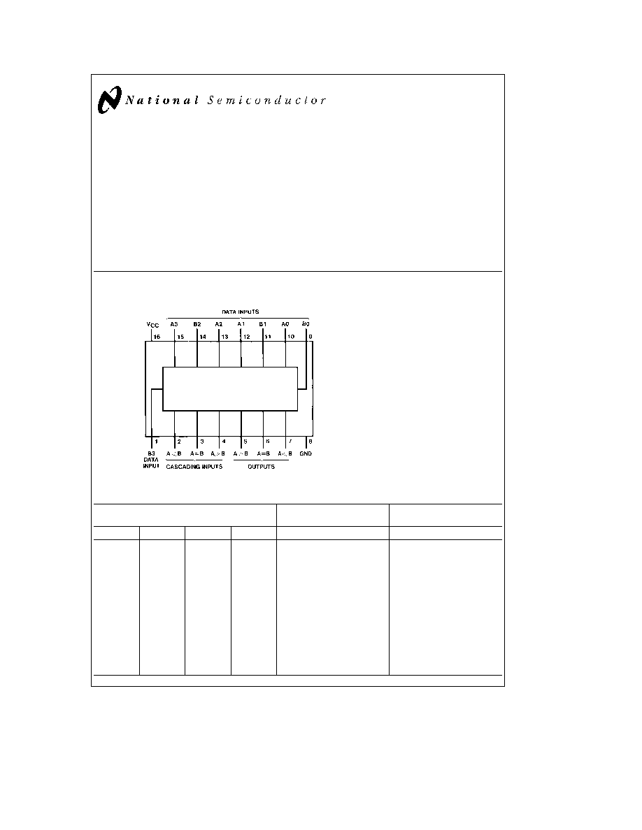
Connection Diagram
Dual-In-Line Package
TL F 6379 � 1
Order Number 54LS85DMQB
54LS85FMQB 54LS85LMQB
DM54LS85J DM54LS85W
DM74LS85M or DM74LS85N
See NS Package Number E20A
J16A M16A N16E or W16A
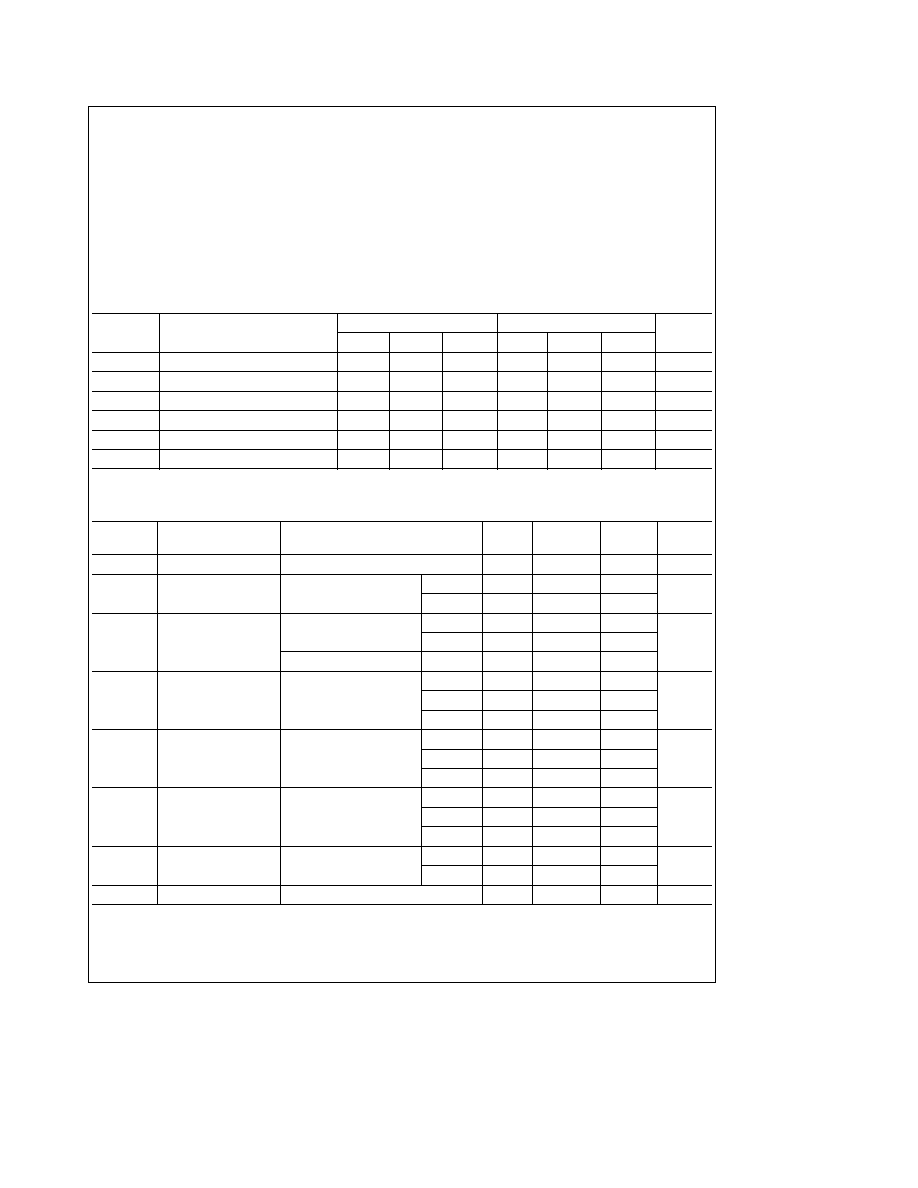
Function Table
Comparing
Cascading
Outputs
Inputs
Inputs
A3 B3
A2 B2
A1 B1
A0 B0
A
l
B
A
k
B
A
e
B
A
l
B
A
k
B
A
e
B
A3
l
B3
X
X
X
X
X
X
H
L
L
A3
k
B3
X
X
X
X
X
X
L
H
L
A3
e
B3
A2
l
B2
X
X
X
X
X
H
L
L
A3
e
B3
A2
k
B2
X
X
X
X
X
L
H
L
A3
e
B3
A2
e
B2
A1
l
B1
X
X
X
X
H
L
L
A3
e
B3
A2
e
B2
A1
k
B1
X
X
X
X
L
H
L
A3
e
B3
A2
e
B2
A1
e
B1
A0
l
B0
X
X
X
H
L
L
A3
e
B3
A2
e
B2
A1
e
B1
A0
k
B0
X
X
X
L
H
L
A3
e
B3
A2
e
B2
A1
e
B1
A0
e
B0
H
L
L
H
L
L
A3
e
B3
A2
e
B2
A1
e
B1
A0
e
B0
L
H
L
L
H
L
A3
e
B3
A2
e
B2
A1
e
B1
A0
e
B0
L
L
H
L
L
H
A3
e
B3
A2
e
B2
A1
e
B1
A0
e
B0
X
X
H
L
L
H
A3
e
B3
A2
e
B2
A1
e
B1
A0
e
B0
H
H
L
L
L
L
A3
e
B3
A2
e
B2
A1
e
B1
A0
e
B0
L
L
L
H
H
L
H
e
High Level L
e
Low Level X
e
Don't Care
C1995 National Semiconductor Corporation
RRD-B30M105 Printed in U S A
Absolute Maximum Ratings
(Note)
If Military Aerospace specified devices are required
please contact the National Semiconductor Sales
Office Distributors for availability and specifications
Supply Voltage
7V
Input Voltage
7V
Operating Free Air Temperature Range
DM54LS and 54LS
b
55 C to
a
125 C
DM74LS
0 C to
a
70 C
Storage Temperature Range
b
65 C to
a
150 C
Note
The ``Absolute Maximum Ratings'' are those values
beyond which the safety of the device cannot be guaran-
teed The device should not be operated at these limits The
parametric values defined in the ``Electrical Characteristics''
table are not guaranteed at the absolute maximum ratings
The ``Recommended Operating Conditions'' table will define
the conditions for actual device operation
Recommended Operating Conditions
Symbol
Parameter
DM54LS85
DM74LS85
Units
Min
Nom
Max
Min
Nom
Max
V
CC
Supply Voltage
4 5
5
5 5
4 75
5
5 25
V
V
IH
High Level Input Voltage
2
2
V
V
IL
Low Level Input Voltage
0 7
0 8
V
I
OH
High Level Output Current
b
0 4
b
0 4
mA
I
OL
Low Level Output Current
4
8
mA
T
A
Free Air Operating Temperature
b
55
125
0
70
C
Electrical Characteristics
over recommended operating free air temperature range (unless otherwise noted)
Symbol
Parameter
Conditions
Min
Typ
Max
Units
(Note 1)
V
I
Input Clamp Voltage
V
CC
e
Min I
I
e b
18 mA
b
1 5
V
V
OH
High Level Output
V
CC
e
Min I
OH
e
Max
DM54
2 5
3 4
V
Voltage
V
IL
e
Max V
IH
e
Min
DM74
2 7
3 4
V
OL
Low Level Output
V
CC
e
Min I
OL
e
Max
DM54
0 25
0 4
Voltage
V
IL
e
Max V
IH
e
Min
DM74
0 35
0 5
V
I
OL
e
4 mA V
CC
e
Min
DM74
0 25
0 4
I
I
Input Current
Max
V
CC
e
Max
A
k
B
0 1
Input Voltage
V
I
e
7V
A
l
B
0 1
mA
Others
0 3
I
IH
High Level Input
V
CC
e
Max
A
k
B
20
Current
V
I
e
2 7V
A
l
B
20
m
A
Others
60
I
IL
Low Level Input
V
CC
e
Max
A
k
B
b
0 4
Current
V
I
e
0 4V
A
l
B
b
0 4
mA
Others
b
1 2
I
OS
Short Circuit
V
CC
e
Max
DM54
b
20
b
100
mA
Output Current
(Note 2)
DM74
b
20
b
100
I
CC
Supply Current
V
CC
e
Max (Note 3)
10
20
mA
Note 1
All typicals are at V
CC
e
5V T
A
e
25 C
Note 2
Not more than one output should be shorted at a time and the duration should not exceed one second
Note 3
I
CC
is measured with all outputs open A
e
B grounded and all other inputs at 4 5V
2
Switching Characteristics
at V
CC
e
5V and T
A
e
25 C (See Section 1 for Test Waveforms and Output Load)
From
To
Number of
R
L
e
2 kX
Symbol
Parameter
Input
Output
Gate Levels
C
L
e
15 pF
C
L
e
50 pF
Units
Min
Max
Min
Max
t
PLH
Propagation Delay Time
Any A or B
A
k
B
3
36
42
Low-to-High Level Output
Data Input
A
l
B
ns
A
e
B
4
40
40
t
PHL
Propagation Delay Time
Any A or B
A
k
B
3
30
40
High-to-Low Level Output
Data Input
A
l
B
ns
A
e
B
4
30
40
t
PLH
Propagation Delay Time
A
k
B
A
l
B
1
22
26
ns
Low-to-High Level Output
or A
e
B
t
PHL
Propagation Delay Time
A
k
B
A
l
B
1
17
26
ns
High-to-Low Level Output
or A
e
B
t
PLH
Propagation Delay Time
A
e
B
A
e
B
2
20
25
ns
Low-to-High Level Output
t
PHL
Propagation Delay Time
A
e
B
A
e
B
2
17
26
ns
High-to-Low Level Output
t
PLH
Propagation Delay Time
A
l
B
A
k
B
1
22
26
ns
Low-to-High Level Output
or A
e
B
t
PHL
Propagation Delay Time
A
l
B
A
k
B
1
17
26
ns
High-to-Low Level Output
or A
e
B
3
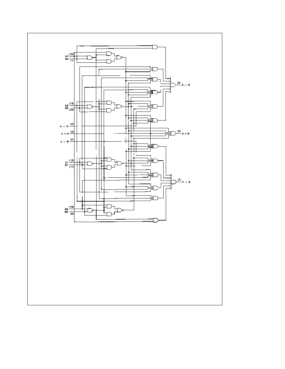
Logic Diagram
TL F 6379 � 2
4

5
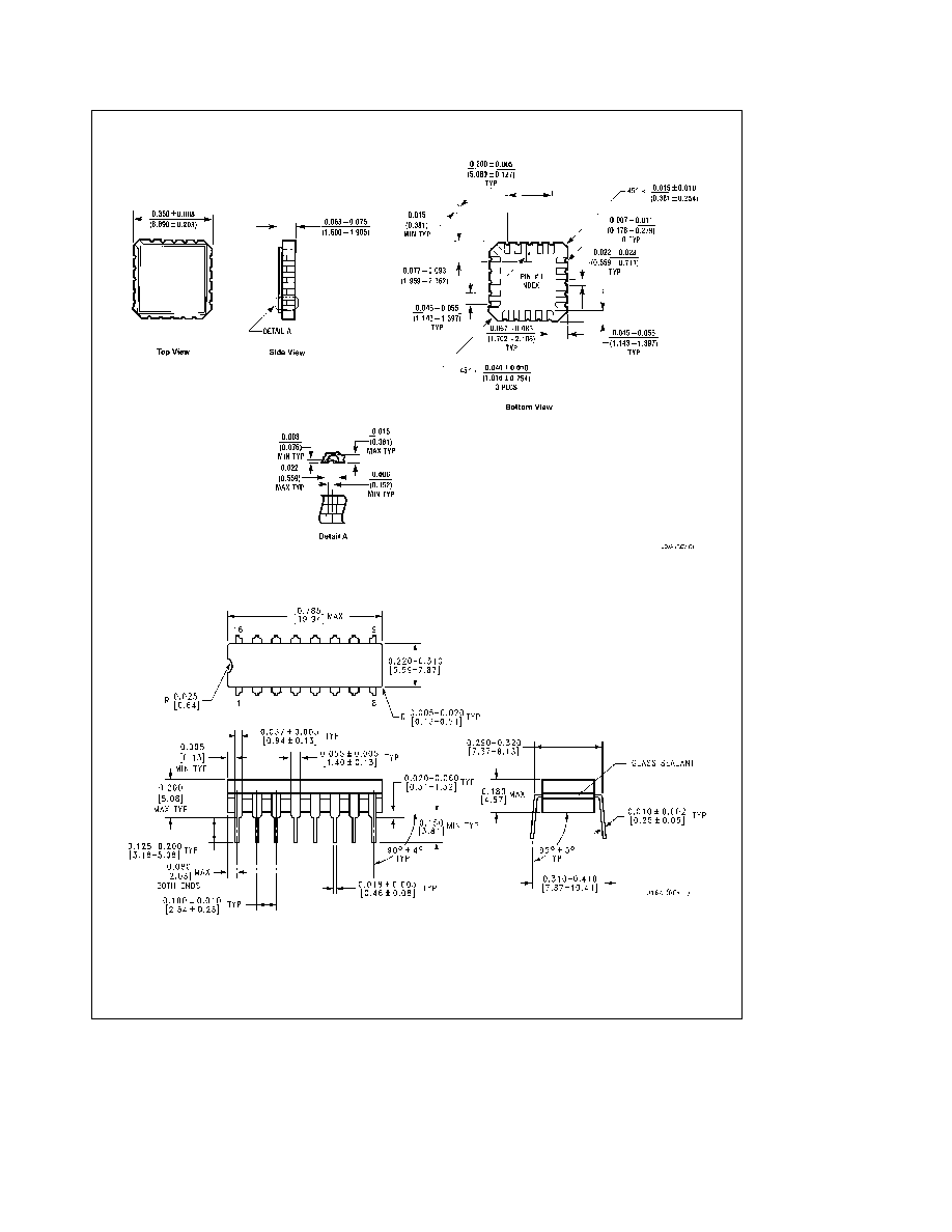
Physical Dimensions
inches (millimeters)
Chip Carrier Package (E)
Order Number 54LS85LMQB
NS Package Number E20A
16-Lead Ceramic Dual-In-Line Package (J)
Order Number 54LS85DMQB or DM54LS85J
NS Package Number J16A
6
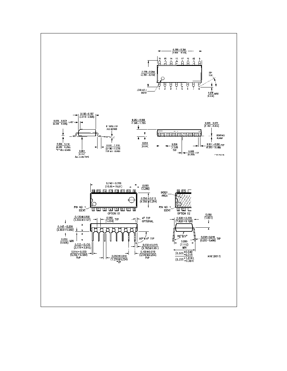
Physical Dimensions
inches (millimeters) (Continued)
16-Lead Small Outline Molded Package (M)
Order Number DM74LS85M
NS Package Number M16A
16-Lead Molded Dual-In-Line Package (N)
Order Number DM74LS85N
NS Package Number N16E
7
54LS85DM54LS85DM74LS85
4-Bit
Magnitude
Comparators
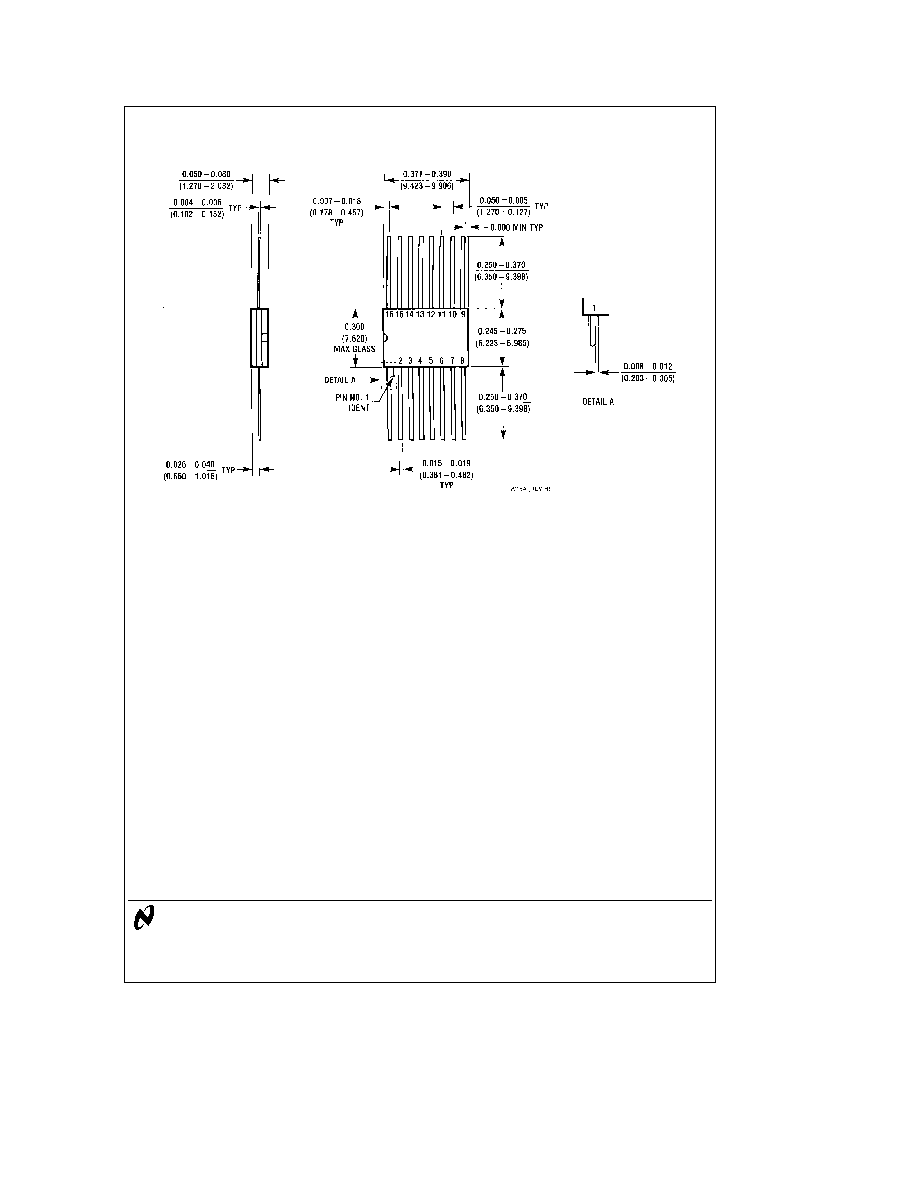
Physical Dimensions
inches (millimeters) (Continued)
16-Lead Ceramic Flat Package (W)
Order Number 54LS85FMQB or DM54LS85W
NS Package Number W16A
LIFE SUPPORT POLICY
NATIONAL'S PRODUCTS ARE NOT AUTHORIZED FOR USE AS CRITICAL COMPONENTS IN LIFE SUPPORT
DEVICES OR SYSTEMS WITHOUT THE EXPRESS WRITTEN APPROVAL OF THE PRESIDENT OF NATIONAL
SEMICONDUCTOR CORPORATION As used herein
1 Life support devices or systems are devices or
2 A critical component is any component of a life
systems which (a) are intended for surgical implant
support device or system whose failure to perform can
into the body or (b) support or sustain life and whose
be reasonably expected to cause the failure of the life
failure to perform when properly used in accordance
support device or system or to affect its safety or
with instructions for use provided in the labeling can
effectiveness
be reasonably expected to result in a significant injury
to the user
National Semiconductor
National Semiconductor
National Semiconductor
National Semiconductor
Corporation
Europe
Hong Kong Ltd
Japan Ltd
1111 West Bardin Road
Fax (a49) 0-180-530 85 86
13th Floor Straight Block
Tel 81-043-299-2309
Arlington TX 76017
Email cnjwge tevm2 nsc com
Ocean Centre 5 Canton Rd
Fax 81-043-299-2408
Tel 1(800) 272-9959
Deutsch Tel (a49) 0-180-530 85 85
Tsimshatsui Kowloon
Fax 1(800) 737-7018
English
Tel (a49) 0-180-532 78 32
Hong Kong
Fran ais Tel (a49) 0-180-532 93 58
Tel (852) 2737-1600
Italiano
Tel (a49) 0-180-534 16 80
Fax (852) 2736-9960
National does not assume any responsibility for use of any circuitry described no circuit patent licenses are implied and National reserves the right at any time without notice to change said circuitry and specifications