TL F 6533
DM5490DM7490A
DM7493A
Decade
and
Binary
Counters
July 1992
DM5490 DM7490A DM7493A
Decade and Binary Counters
General Description
Each of these monolithic counters contains four master-
slave flip-flops and additional gating to provide a divide-by-
two counter and a three-stage binary counter for which the
count cycle length is divide-by-five for the 90A and divide-
by-eight for the 93A
All of these counters have a gated zero reset and the 90A
also has gated set-to-nine inputs for use in BCD nine's com-
plement applications
To use their maximum count length (decade or four-bit bina-
ry) the B input is connected to the Q
A
output The input
count pulses are applied to input A and the outputs are as
described in the appropriate truth table A symmetrical di-
vide-by-ten count can be obtained from the 90A counters by
connecting the Q
D
output to the A input and applying the
input count to the B input which gives a divide-by-ten square
wave at output Q
A
Features
Y
Typical power dissipation
90A
145 mW
93A
130 mW
Y
Count frequency 42 MHz
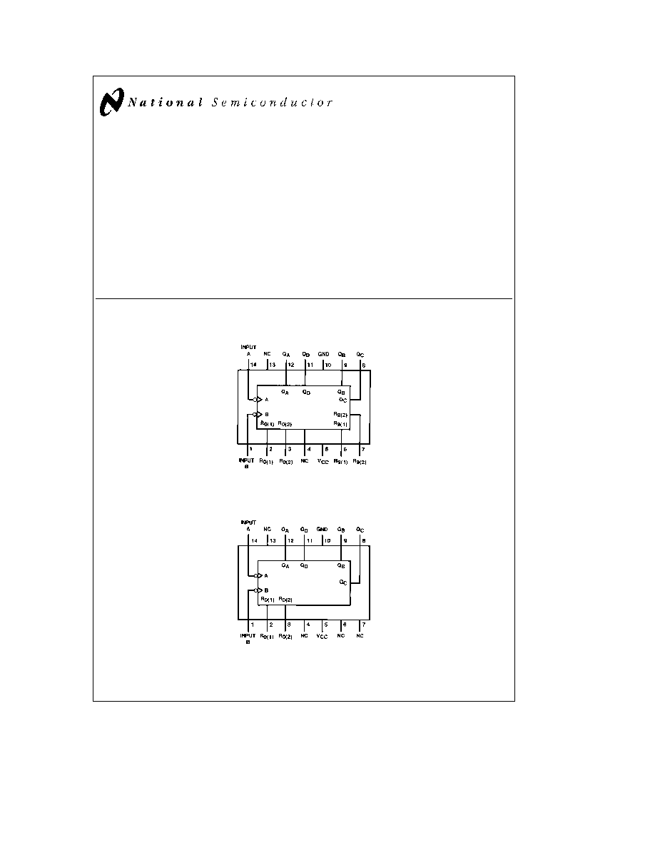
Connection Diagrams
Dual-In-Line Package
TL F 6533 � 1
Order Number DM5490J DM5490W or DM7490AN
See NS Package Number J14A N14A or W14B
Dual-In-Line Package
TL F 6533 � 2
Order Number DM7493AN
See NS Package Number N14A
C1995 National Semiconductor Corporation
RRD-B30M105 Printed in U S A
Absolute Maximum Ratings
(Note)
If Military Aerospace specified devices are required
please contact the National Semiconductor Sales
Office Distributors for availability and specifications
Supply Voltage
7V
Input Voltage
5 5V
Operating Free Air Temperature Range
DM54
b
55 C to
a
125 C
DM74
0 C to
a
70 C
Storage Temperature Range
b
65 C to
a
150 C
Note
The ``Absolute Maximum Ratings'' are those values
beyond which the safety of the device cannot be guaran-
teed The device should not be operated at these limits The
parametric values defined in the ``Electrical Characteristics''
table are not guaranteed at the absolute maximum ratings
The ``Recommended Operating Conditions'' table will define
the conditions for actual device operation
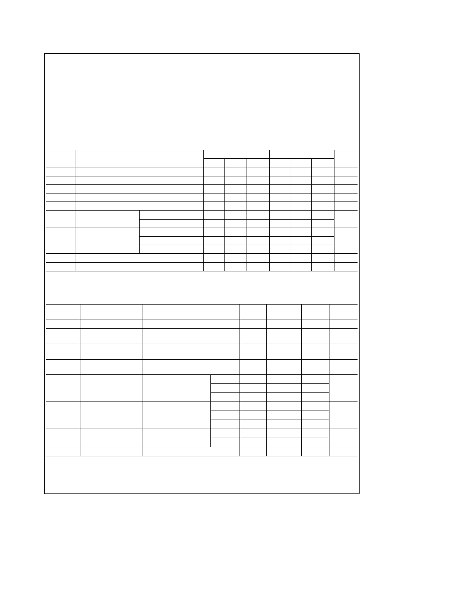
Recommended Operating Conditions
Symbol
Parameter
DM5490
DM7490A
Units
Min
Nom
Max
Min
Nom
Max
V
CC
Supply Voltage
4 5
5
5 5
4 75
5
5 25
V
V
IH
High Level Input Voltage
2
2
V
V
IL
Low Level Input Voltage
0 8
0 8
V
I
OH
High Level Output Current
b
0 8
b
0 8
mA
I
OL
Low Level Output Current
16
16
mA
f
CLK
Clock Frequency
A
0
32
0
32
MHz
(Note 5)
B
0
16
0
16
t
W
Pulse Width
A
15
15
(Note 5)
B
30
30
ns
Reset
15
15
t
REL
Reset Release Time (Note 5)
25
25
ns
T
A
Free Air Operating Temperature
b
55
125
0
70
C
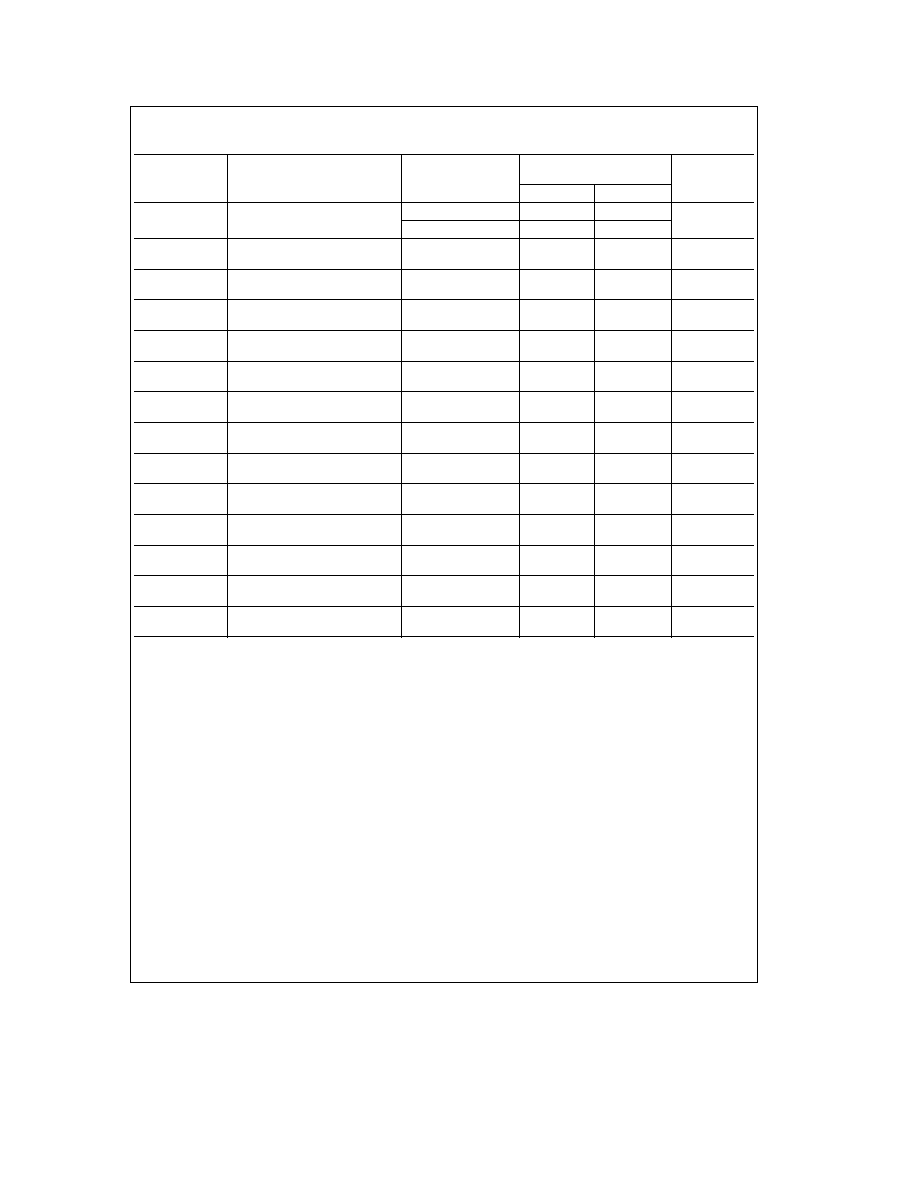
'90A Electrical Characteristics
over recommended operating free air temperature range (unless otherwise noted)
Symbol
Parameter
Conditions
Min
Typ
Max
Units
(Note 1)
V
I
Input Clamp Voltage
V
CC
e
Min I
I
e b
12 mA
b
1 5
V
V
OH
High Level Output
V
CC
e
Min I
OH
e
Max
2 4
3 4
V
Voltage
V
IL
e
Max V
IH
e
Min
V
OL
Low Level Output
V
CC
e
Min I
OL
e
Max
0 2
0 4
V
Voltage
V
IH
e
Min V
IL
e
Max (Note 4)
I
I
Input Current
Max
V
CC
e
Max V
I
e
5 5V
1
mA
Input Voltage
I
IH
High Level Input
V
CC
e
Max
A
80
Current
V
I
e
2 7V
Reset
40
m
A
B
120
I
IL
Low Level Input
V
CC
e
Max
A
b
3 2
Current
V
I
e
0 4V
Reset
b
1 6
mA
B
b
4 8
I
OS
Short Circuit
V
CC
e
Max
DM54
b
20
b
57
mA
Output Current
(Note 2)
DM74
b
18
b
57
I
CC
Supply Current
V
CC
e
Max (Note 3)
29
42
mA
Note 1
All typicals are at V
CC
e
5V T
A
e
25 C
Note 2
Not more than one output should be shorted at a time
Note 3
I
CC
is measured with all outputs open both RO inputs grounded following momentary connection to 4 5V and all other inputs grounded
Note 4
Q
A
outputs are tested at I
OL
e
Max plus the limit value of I
IL
for the B input This permits driving the B input while maintaining full fan-out capability
Note 5
T
A
e
25 C and V
CC
e
5V
2
'90A Switching Characteristics
at V
CC
e
5V and T
A
e
25 C (See Section 1 for Test Waveforms and Output Load)
From (Input)
R
L
e
400X
Symbol
Parameter
To (Output)
C
L
e
15 pF
Units
Min
Max
f
MAX
Maximum Clock
A to Q
A
32
MHz
Frequency
B to Q
B
16
t
PLH
Propagation Delay Time
A to Q
A
16
ns
Low to High Level Output
t
PHL
Propagation Delay Time
A to Q
A
18
ns
High to Low Level Output
t
PLH
Propagation Delay Time
A to Q
D
48
ns
Low to High Level Output
t
PHL
Propagation Delay Time
A to Q
D
50
ns
High to Low Level Output
t
PLH
Propagation Delay Time
B to Q
B
16
ns
Low to High Level Output
t
PHL
Propagation Delay Time
B to Q
B
21
ns
High to Low Level Output
t
PLH
Propagation Delay Time
B to Q
C
32
ns
Low to High Level Output
t
PHL
Propagation Delay Time
B to Q
C
35
ns
High to Low Level Output
t
PLH
Propagation Delay Time
B to Q
D
32
ns
Low to High Level Output
t
PHL
Propagation Delay Time
B to Q
D
35
ns
High to Low Level Output
t
PLH
Propagation Delay Time
SET-9 to
30
ns
Low to High Level Output
Q
A
Q
D
t
PHL
Propagation Delay Time
SET-9 to
40
ns
High to Low Level Output
Q
B
Q
C
t
PHL
Propagation Delay Time
SET-0
40
ns
High to Low Level Output
Any Q
3

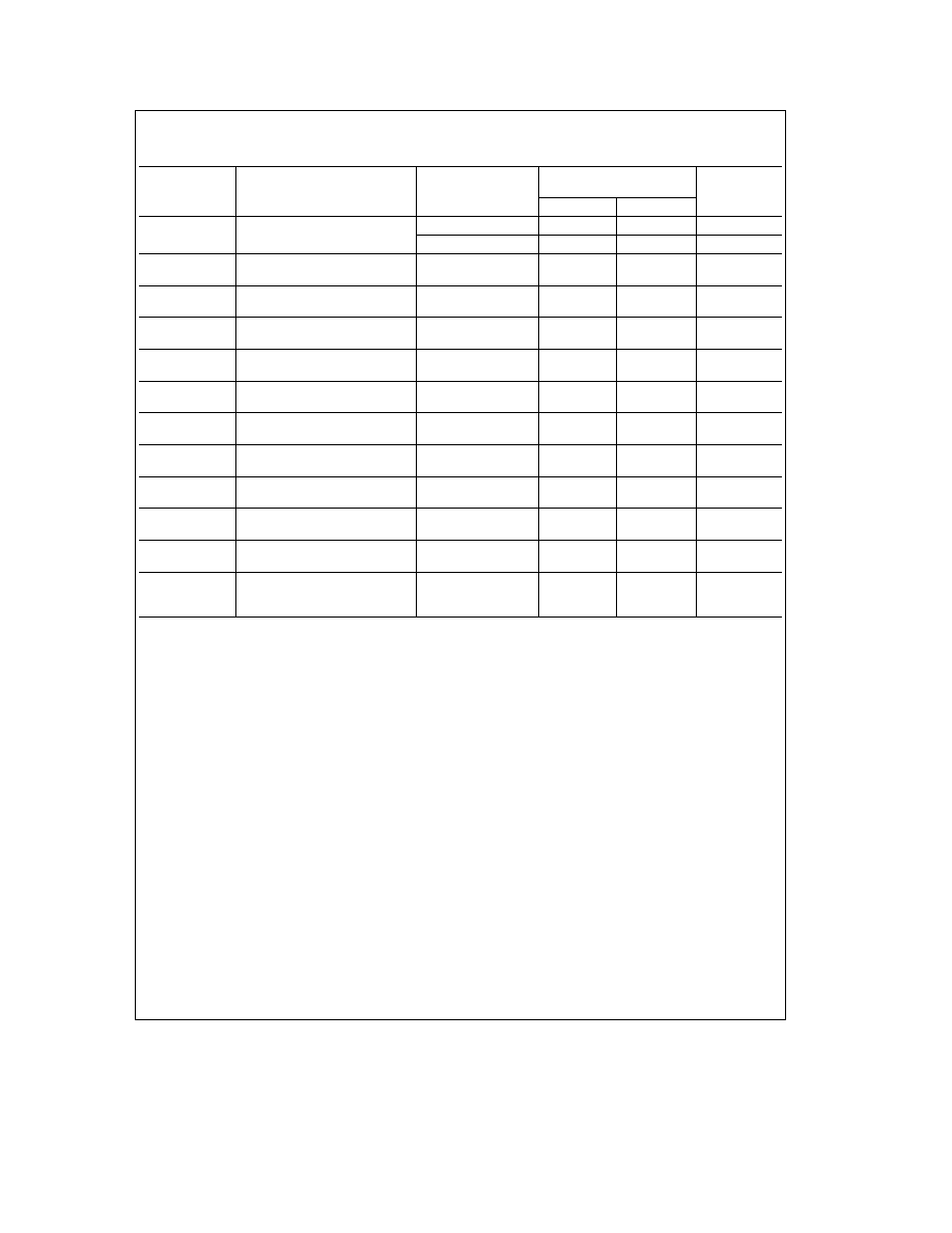
Recommended Operating Conditions
Symbol
Parameter
DM7493A
Units
Min
Nom
Max
V
CC
Supply Voltage
4 75
5
5 25
V
V
IH
High Level Input Voltage
2
V
V
IL
Low Level Input Voltage
0 8
V
I
OH
High Level Output Current
b
0 8
mA
I
OL
Low Level Output Current
16
mA
f
CLK
Clock Frequency
A
0
32
MHz
(Note 5)
B
0
16
t
W
Pulse Width
A
15
(Note 5)
B
30
ns
Reset
15
t
REL
Reset Release Time (Note 5)
25
ns
T
A
Free Air Operating Temperature
0
70
C
'93A Electrical Characteristics
over recommended operating free air temperature range (unless otherwise noted)
Symbol
Parameter
Conditions
Min
Typ
Max
Units
(Note 1)
V
I
Input Clamp Voltage
V
CC
e
Min I
I
e b
12 mA
b
1 5
V
V
OH
High Level Output
V
CC
e
Min I
OH
e
Max
2 4
3 4
V
Voltage
V
IL
e
Max V
IH
e
Min
V
OL
Low Level Output
V
CC
e
Min I
OL
e
Max
0 2
0 4
V
Voltage
V
IH
e
Min V
IL
e
Max (Note 4)
I
I
Input Current
Max
V
CC
e
Max V
I
e
5 5V
1
mA
Input Voltage
I
IH
High Level Input
V
CC
e
Max
Reset
40
Current
V
I
e
2 4V
A
80
m
A
B
80
I
IL
Low Level Input
V
CC
e
Max
Reset
b
1 6
Current
V
I
e
0 4V
A
b
3 2
mA
B
b
3 2
I
OS
Short Circuit
V
CC
e
Max
b
18
b
57
mA
Output Current
(Note 2)
I
CC
Supply Current
V
CC
e
Max (Note 3)
26
39
mA
Note 1
All typicals are at V
CC
e
5V T
A
e
25 C
Note 2
Not more than one output should be shorted at a time
Note 3
I
CC
is measured with all outputs open both R0 inputs grounded following momentary connection to 4 5V and all other inputs grounded
Note 4
Q
A
outputs are tested at I
OL
e
Max plus the limit value of I
IL
for the B input This permits driving the B input while maintaining full fan-out capability
Note 5
T
A
e
25 C and V
CC
e
5V
4
'93A Switching Characteristics
at V
CC
e
5V and T
A
e
25 C (See Section 1 for Test Waveforms and Output Load)
From (Input)
R
L
e
400X
Symbol
Parameter
To (Output)
C
L
e
15 pF
Units
Min
Max
f
MAX
Maximum Clock
A to Q
A
32
MHz
Frequency
B to Q
B
16
t
PLH
Propagation Delay Time
A to
16
ns
Low to High Level Output
Q
A
t
PHL
Propagation Delay Time
A to
18
ns
High to Low Level Output
Q
A
t
PLH
Propagation Delay Time
A to
70
ns
Low to High Level Output
Q
D
t
PHL
Propagation Delay Time
A to
70
ns
High to Low Level Output
Q
D
t
PLH
Propagation Delay Time
B to
16
ns
Low to High Level Output
Q
B
t
PHL
Propagation Delay Time
B to
21
ns
High to Low Level Output
Q
B
t
PLH
Propagation Delay Time
B to
32
ns
Low to High Level Output
Q
C
t
PHL
Propagation Delay Time
B to
35
ns
High to Low Level Output
Q
C
t
PLH
Propagation Delay Time
B to
51
ns
Low to High Level Output
Q
D
t
PHL
Propagation Delay Time
B to
51
ns
High to Low Level Output
Q
D
t
PHL
Propagation Delay Time
SET-0
High to Low Level Output
to
40
ns
Any Q
5