TL F 11654
5474ETL16245
16-Bit
Data
Transceiver
with
Incident
Wave
Switching
PRELIMINARY
May 1994
54 74ETL16245 16-Bit Data
Transceiver with Incident Wave Switching
General Description
The 54 74ETL16245 contains sixteen non-inverting bidirec-
tional buffers with TRI-STATE
outputs designed with inci-
dent wave switching live insertion support and enhanced
noise margin for TTL backplane applications
Both the A and B ports include a bus hold circuit to latch the
output to the value last forced on that pin
The B port of this device includes 25X series output resis-
tors which minimize undershoot and ringing
Features
Y
Supports the VME64 ETL specification
Y
Functionally and pin compatible with industry standard
TTL 16245 SSOP pinout
Y
Improved TTL-compatible input threshold range
Y
High drive TTL-compatible outputs (I
OH
e
b
60 mA
I
OL
e
90 mA)
Y
Supports 25X incident wave switching on the A port
Y
BiCMOS design significantly reduces power dissipation
Y
Distributed V
CC
and GND pin configuration minimizes
high-speed switching noise
Y
25X series-dampening resistor on B-port
Y
Available in 48-pin SSOP and ceramic flatpak
Y
Guaranteed output skew
Y
Guaranteed simultaneous switching noise level and
dynamic threshold performance
Y
Guaranteed latchup protection
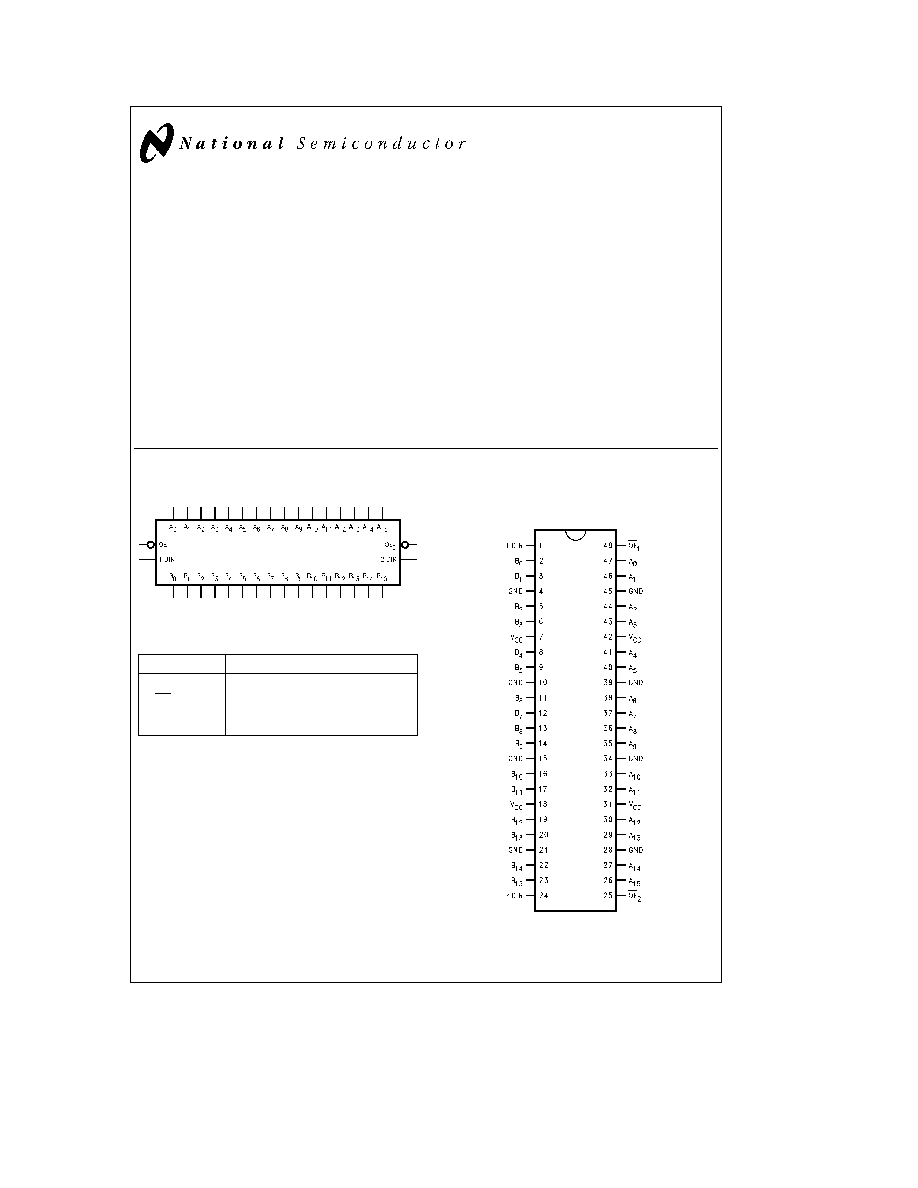
Logic Symbol
TL F 11654 � 1
Pin Description
Pin Names
Description
DIR
Transmit Receive Input
OE
Output Enable Input (Active LOW)
A
n
Backplane Bus Data
B
n
Local Bus Data
Connection Diagram
Pin Assignment for
SSOP and Flatpak
TL F 11654 � 2
TRI-STATE
is a registered trademark of National Semiconductor Corporation
C1995 National Semiconductor Corporation
RRD-B30M105 Printed in U S A
Functional Description
The device uses byte-wide Direction (DIR) control and Out-
put Enable (OE) controls The DIR inputs determine the di-
rection of data flow through the device The OE inputs dis-
able the A and the B ports
The part contains active circuitry which keeps all outputs
disabled when V
CC
is less than 2 2V to aid in live insertion
applications
Truth Table
(Each 8-bit Section)
Inputs
Operation
OE
DIR
L
L
A Data to B Bus
L
H
B Data to A Bus
H
X
Isolation
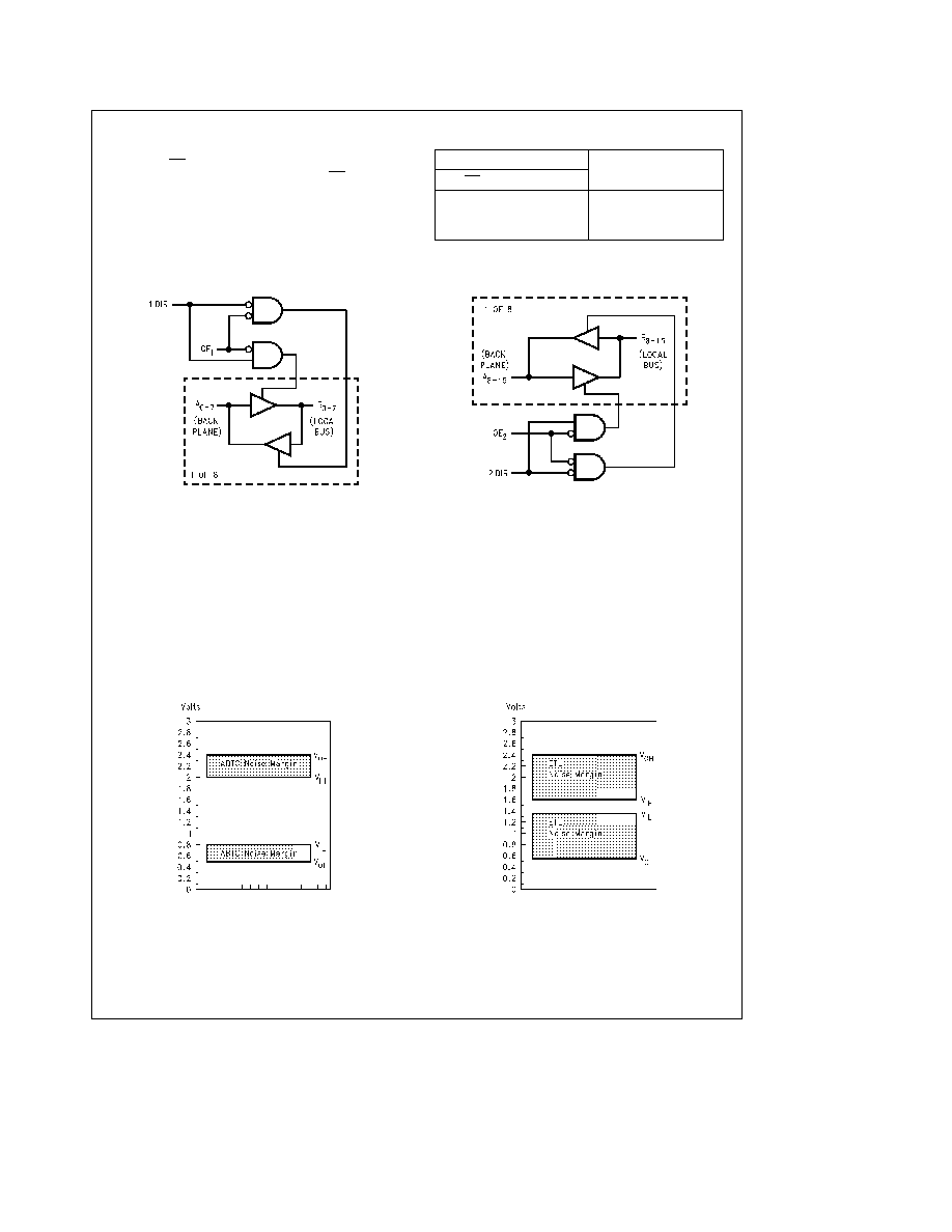
Logic Diagrams
(Positive Logic)
TL F 11654 � 3
TL F 11654 � 4
ETL's Improved Noise Immunity
TTL input thresholds are typically determined by tempera-
ture-dependent junction voltages which result in worst case
input thresholds between 0 8V and 2 0V By contrast ETL
provides greater noise immunity because its input thresh-
olds are determined by current mode input circuits similar to
those used for ECL or BTL ETL's worst case input thresh-
olds between 1 4V and 1 6V are compensated for temper-
ature voltage and process variations
Incident Wave Switching
When TTL logic is used to drive fully loaded backplanes the
combination of low backplane bus characteristic imped-
ance wide TTL input threshold range and limited TTL drive
generally require multiple waveform reflections before a val-
id signal can be received across the backplane The VME
International Trade Association (VITA) defined ETL to pro-
vide incident wave switching which increases the data trans-
fer rate of a VME backplane and extends the life of VME
applications TTL compatibility with existing VME back-
planes and modules was maintained
Improved Input Threshold Characteristics of ETL
TL F 11654 � 5
ABTC Worst Case V
OUT
� V
IN
TL F 11654 � 6
ETL Worst Case V
OUT
� V
IN
2

Incident Wave Switching
(Continued)
To demonstrate the incident wave switching capability con-
sider a VME application A VME bus must be terminated to
a
2 94V with 190X at each end of its 21 card backplane
The surge impedance presented by a fully loaded VME
backplane is approximately 25X If the output voltage cur-
rent of an ABTC driver is plotted with this load the inter-
section at 1 2V for a falling edge and at 1 6V for a rising
edge does not reach the worst case input threshold of a
second ABTC circuit This is shown in the two figures below
However an ETL driver located at one end of the backplane
is able to provide incident wave switching because it has a
higher drive and a tighter input threshold
Estimated ETL ABTC Initial Falling Edge Step
TL F 11654 � 7
Because ETL has a much more precise input threshold re-
gion an ETL receiver will interpret its predicted falling input
of 0 85V as a logic ZERO and the initial rising edge of 1 9V
as a logic ONE This comparison is for the case of a 25X
surge impedance backplane driven from one end
Estimated ETL ABTC Initial Rising Edge Step
TL F 11654 � 8
The resulting ABTC and ETL waveform predictions and their input thresholds are compared below This shows how ETL can
achieve backplane speeds not always possible with conventional TTL compatible logic families
Comparing the Incident Wave Switching of ETL with ABTC
TL F 11654 � 9
3

Incident Wave Switching
(Continued)
The figure V
CC
Power-up Critical Voltages shows the rela-
tionship between OE and V
CC
while power is being applied
and removed
TL F 11654 � 10
V
CC
and OE Power-up Relationship
4

Absolute Maximum Ratings
(Note 1)
If Military Aerospace specified devices are required
please contact the National Semiconductor Sales
Office Distributors for availability and specifications
Storage Temperature
b
65 C to
a
150 C
Ambient Temperature under Bias
b
55 C to
a
125 C
Junction Temperature under Bias
Ceramic
b
55 C to
a
175 C
Plastic
b
55 C to
a
150 C
V
CC
Pin Potential to
Ground Pin
b
0 5V to
a
7 0V
Input Voltage (Note 2)
b
0 5V to
a
7 0V
Input Current (Note 2)
b
50 mA to
a
5 0 mA
Voltage Applied to Any Output
in the Disabled or
Power-off State
b
0 5V to 5 5V
in the HIGH State
b
0 5V to V
CC
Current Applied to Output
in LOW State (Max)
128 mA
DC Latchup Source Current
b
500 mA
Over Voltage Latchup (I O)
10V
Note 1
Absolute maximum ratings are values beyond which the device may
be damaged or have its useful life impaired Functional operation under
these conditions is not implied
Note 2
Either voltage limit or current limit is sufficient to protect inputs
Recommended Operating
Conditions
Free Air Ambient Temperature
Military
b
55 C to
a
125 C
Commercial
b
40 C to
a
85 C
Supply Voltage
Military
a
4 5V to
a
5 5V
Commercial
a
4 5V to
a
5 5V
Minimum Input Edge Rate
(Dt DV)
Data Input
20 ns V
Enable Input
50 ns V
DC Electrical Characteristics
Symbol
Parameter
ETL16245
Units
V
CC
Conditions
Min
Typ
Max
V
IH
Input HIGH Voltage
OE
2 0
V
Recognized HIGH Signal
Other Inputs
1 6
V
IL
Input LOW Voltage
OE
0 8
V
Recognized LOW Signal
Other Inputs
1 4
V
CD
Input Clamp Diode Voltage
b
1 2
V
Min
I
IN
e b
18 mA (OE
n
DIR)
V
OH
Output HIGH Voltage
V
CC
b
1
V
I
OH
e b
100 mA
B Port
2 4
V
Min
I
OH
e b
1 mA
2 0
V
I
OH
e b
12 mA
V
CC
b
1
V
I
OH
e b
1 mA
A Port
2 4
V
Min
I
OH
e b
32 mA
2 0
V
I
OH
e b
60 mA
V
OL
Output LOW Voltage
B Port
0 4
V
Min
I
OL
e
1 mA
0 8
V
I
OL
e
12 mA
A Port
0 55
V
Min
I
OL
e
64 mA
0 9
V
I
OL
e
90 mA
I
HOLD
Bus Hold Current
B Port
A Port
100
m
A
Min
OE
e
HIGH
V
O
e
0 8V
b
100
OE
e
HIGH
V
O
e
2 0V
I
OFF
Output Current Power Down
100
m
A
0 0
V
CC
Bias
e
0V
V
I
or V
O
s
4 5V
I
I
Input Current Control Pins
54ETL
g
10
m
A
5 5
V
IN
e
0 or V
CC
74ETL
g
5
m
A
5 5
V
IN
e
0 or V
CC
I
IH
a
Output Leakage Current
50
m
A
5 5
V
OUT
e
2 7V OE
e
2 0V
I
OZH
I
IL
a
Output Leakage Current
b
50
m
A
5 5
V
OUT
e
0 5V OE
e
2 0V
I
OZL
5
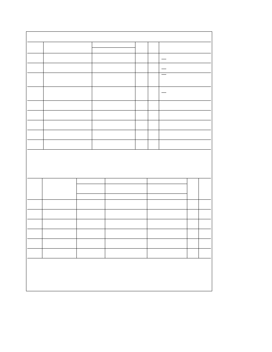
DC Electrical Characteristics
(Continued)
Symbol
Parameter
ETL16245
Units
V
CC
Conditions
Min
Typ
Max
I
CCH
Power Supply Current
40
mA
Max
All Outputs HIGH
OE
e
LOW DIR
e
HIGH or LOW
I
CCL
Power Supply Current
80
mA
Max
All Outputs LOW
OE
e
LOW DIR
e
HIGH or LOW
I
CCZ
Power Supply Current
OE
e
HIGH
40
mA
Max
All Others at V
CC
or GND
DIR
e
HIGH or LOW
I
CCD
Dynamic I
CC
0 15
MHz
mA
Max
Outputs Open
No Load
OE
n
e
GND DIR
e
HIGH
(Note 1)
One Bit Toggling 50% Duty Cycle
V
OLP
Quiet Output Maximum
1 0
V
5 0
T
A
e
25 C (Note 2)
Dynamic V
OL
C
L
e
50 pF R
L
e
500X
V
OLV
Quiet Output Minimum
b
1 4
V
5 0
T
A
e
25 C (Note 2)
Dynamic V
OL
C
L
e
50 pF R
L
e
500X
V
OHV
Minimum High Level Dynamic
2 7
V
5 0
T
A
e
25 C (Note 4)
Output Voltage (Note 1)
C
L
e
50 pF R
L
e
500X
V
IHD
Minimum High Level Dynamic
2 0
1 5
V
5 0
T
A
e
25 C (Note 3)
Input Voltage (Note 1)
C
L
e
50 pF R
L
e
500X
V
ILD
Maximum Low Level Dynamic
1 2
0 8
V
5 0
T
A
e
25 C (Note 3)
Input Voltage (Note 1)
C
L
e
50 pF R
L
e
500X
Note 1
Guaranteed but not tested
Note 2
Max number of outputs defined as (n) n
b
1 data inputs are driven 0V to 3V One output at LOW Guaranteed but not tested
Note 3
Max number of data inputs (n) switching n
b
1 inputs switching 0V to 3V Input-under-test switching 3V to threshold (V
ILD
) 0V to threshold (V
IHD
)
Guaranteed but not tested
Note 4
Max number of outputs defined as (n) n
b
1 data inputs are driven 0V to 3V One output HIGH Guaranteed but not tested
AC Electrical Characteristics
Symbol
Parameter
74ETL
54ETL
74ETL
Units
Fig
No
T
A
e a
25 C
T
A
e b
55 C to
a
125 C
T
A
e b
40 C to
a
85 C
V
CC
e a
5V
V
CC
e
4 5V � 5 5V
V
CC
e
4 5V � 5 5V
Min
Typ
Max
Min
Max
Min
Max
t
PLH
Propagation
1 5
7 0
1 5
7 0
ns
1 2 4
t
PHL
Delay A
n
to B
n
1 5
7 0
1 5
7 0
t
PLH
Propagation
1 5
7 0
1 5
7 0
ns
1 2 4
t
PHL
Delay B
n
to A
n
1 5
7 0
1 5
7 0
t
PZH
Output Enable
1 0
7 0
1 0
7 0
ns
1 2 3
t
PZL
Time
1 0
7 0
1 0
7 0
t
PHZ
Output Disable
1 0
7 0
1 0
7 0
ns
1 2 3
t
PLZ
Time
1 0
7 0
1 0
7 0
t
r
Rise Time 1V
x
2V
1 2
3 0
1 2
3 0
ns
1 2 4
A
n
Outputs
t
f
Fall Time 2V
x
1V
1 2
3 0
1 2
3 0
ns
1 2 4
A
n
Outputs
6

Skew
Symbol
Parameter
74ETL
54ETL
Units
Conditions
T
A
e b
40 C to
a
85 C
T
A
e b
55 C to
a
125 C
V
CC
e
4 5V � 5 5V
V
CC
e
4 5V � 5 5V
16 Outputs Switching
16 Outputs Switching
Max
Max
t
OHS
Pin-to-Pin Skew
1 3
ns
Figures 1 2 4
(Notes 1 2)
LH HL An to Bn
t
OHS
Pin-to-Pin Skew
1 3
ns
Figures 1 2 4
(Notes 1 2)
LH HL Bn to An
t
PS
Duty Cycle Skew
2 0
ns
Figures 1 2 4
(Notes 1 2)
Bn to An
t
PS
Duty Cycle Skew
2 0
ns
Figures 1 2 4
(Notes 1 2)
An to Bn
VME Extended Skew
Symbol
Parameter
74ETL
54ETL
Units
Conditions
T
A
e b
40 C to
a
85 C
T
A
e b
55 C to
a
125 C
V
CC
e
4 5V � 5 5V
V
CC
e
4 5V � 5 5V
16 Outputs Switching
16 Outputs Switching
Max
Max
t
PV
Device-to-Device Skew LH HL
4 0
ns
Figures 1 2 4
(Notes 1 2)
Transitions Bn to An
t
CP
Device-to-Device Skew LH HL
2 5
ns
Figures 1 2 4
(Notes 1 2)
Transitions An to Bn
t
CP
Change in Propagation Delay
4 0
ns
Figures 1 2 4
(Note 1 3)
with Load Bn to An
t
CPV
Device-to-Device Change
(Notes 1 2 3)
in Propagation Delay with
6 0
ns
Figures 1 2 4
with Load Bn to An
Note 1
Skew is defined as the absolute difference in delay between two outputs The specification applies to any outputs switching HIGH to LOW LOW to HIGH
or any combination switching HIGH-to-LOW or LOW-to-HIGH This specification is guaranteed but not tested
Note 2
This is measured with both devices at the same value of V
CC
g
1% and with package temperature differences of 20 C from each other
Note 3
This is measured with Rx in
Figure 1 at 13X for one unit and at 56X for the other unit
Capacitance
Symbol
Parameter
Typ
Max
Units
Conditions T
A
e
25 C
C
IN
Input Capacitance
5
8
pF
V
CC
e
0 0V (OE
n
DIR)
C
I O
(Note 1)
Output Capacitance
9
12
pF
V
CC
e
5 0V (A
n
)
Note 1
C
I O
is measured at frequency f
e
1 MHz per MIL-STD-883B Method 3012
7
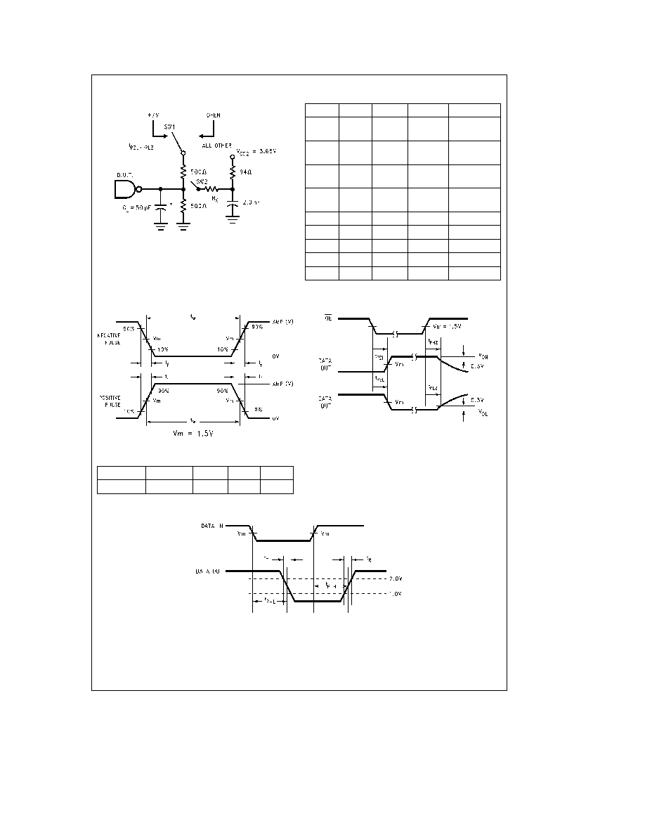
AC Loading
TL F 11654 � 11
Includes jig and probe capacitance
FIGURE 1 Standard AC Test Load
Note 1
Defined to emulate the range of VME bus transmission line loading
as a function of board population and driver location Rx
e
13X 26X or
56X depending on test
Test
Port
SW1
SW2
Rx
t
PHZ
A B
a
7
Open
t
PLZ
t
PZH
A B
a
7
Open
t
PZL
t
PLH
A
Open
Closed
26
t
PHL
t
PLH
B
Open
Open
t
PHL
t
r
t
f
A
Open
Closed
26
t
PV
A
Open
Closed
26
t
CP
B
Open
Open
t
CP
A
Open
Closed
13 then 56
t
CPV
A
Open
Closed
13 and 56
FIGURE 1a
TL F 11654 � 12
FIGURE 2 Input Pulse Requirements
Amplitude
Rep Rate
t
w
t
r
t
f
3 0V
1 MHz
500 ns
2 5 ns
2 5 ns
FIGURE 2a Test Input Signal Requirements
TL F 11654 � 13
FIGURE 3 TRI-STATE Output HIGH
and LOW Enable and Disable Times
TL F 11654 � 14
FIGURE 4 Rise Fall Time and Propagation Delay Waveforms
8
Ordering Information
The device number is used to form part of a simplified purchasing code where the package type and temperature range are
defined as follows
54 74
ETL16245
SS
C
X
Temperature Range Family
Special Variations
VME74
e
Commercial
X
e
Devices shipped in 13 reels
VME54
e
Military
QB
e
Military grade device with
environmental and burn-in
Device Type
processing shipped in tubes
Package Code
Temperature Range
SS
e
Small Outline (SSOP)
C
e
Commercial
FPFP
e
Fine Pitch Flatpak
(
b
40 C to
a
85 C)
M
e
Military (
b
55 C to
a
125 C)
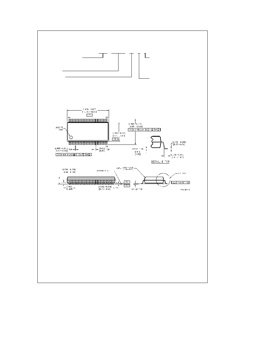
Physical Dimensions
inches (millimeters)
48-Lead SSOP (0 300 Wide) (SS)
NS Package Number MS48A
9

5474ETL16245
16-Bit
Data
Transceiver
with
Incident
Wave
Switching
Physical Dimensions
inches (millimeters) (Continued)
48-Pin Ceramic Flatpak (FPFP)
NS Package Number WA48A
LIFE SUPPORT POLICY
NATIONAL'S PRODUCTS ARE NOT AUTHORIZED FOR USE AS CRITICAL COMPONENTS IN LIFE SUPPORT
DEVICES OR SYSTEMS WITHOUT THE EXPRESS WRITTEN APPROVAL OF THE PRESIDENT OF NATIONAL
SEMICONDUCTOR CORPORATION As used herein
1 Life support devices or systems are devices or
2 A critical component is any component of a life
systems which (a) are intended for surgical implant
support device or system whose failure to perform can
into the body or (b) support or sustain life and whose
be reasonably expected to cause the failure of the life
failure to perform when properly used in accordance
support device or system or to affect its safety or
with instructions for use provided in the labeling can
effectiveness
be reasonably expected to result in a significant injury
to the user
National Semiconductor
National Semiconductor
National Semiconductor
National Semiconductor
Corporation
Europe
Hong Kong Ltd
Japan Ltd
1111 West Bardin Road
Fax (a49) 0-180-530 85 86
13th Floor Straight Block
Tel 81-043-299-2309
Arlington TX 76017
Email cnjwge tevm2 nsc com
Ocean Centre 5 Canton Rd
Fax 81-043-299-2408
Tel 1(800) 272-9959
Deutsch Tel (a49) 0-180-530 85 85
Tsimshatsui Kowloon
Fax 1(800) 737-7018
English
Tel (a49) 0-180-532 78 32
Hong Kong
Fran ais Tel (a49) 0-180-532 93 58
Tel (852) 2737-1600
Italiano
Tel (a49) 0-180-534 16 80
Fax (852) 2736-9960
National does not assume any responsibility for use of any circuitry described no circuit patent licenses are implied and National reserves the right at any time without notice to change said circuitry and specifications