
TL F 10665
74FCT534
Octal
D
Flip-Flop
with
TRI-STATE
Outputs
April 1993
74FCT534
Octal D Flip-Flop with TRI-STATE
Outputs
General Description
The 'FCT534 is a high-speed low-power octal D-type flip-
flop featuring separate D-type inputs for each flip-flop and
TRI-STATE outputs for bus-oriented applications A buff-
ered Clock (CP) and Output Enable (OE) are common to all
flip-flops FACT
TM
FCT utilizes NSC quiet series technology
to provide improved quiet output switching and dynamic
threshold performance
FACT FCT features GTO
TM
output control and undershoot
corrector in addition to a split ground bus for superior per-
formance The 'FCT534 is the same as the 'FCT374 except
that the outputs are inverted
Features
Y
I
CC
and I
OZ
reduced to 40 0 mA and
g
2 5 mA
respectively
Y
NSC 54 74FCT534 is pin and functionally equivalent to
IDT 54 74FCT534
Y
Edge-triggered D-type inputs
Y
Buffered positive edge-triggered clock
Y
Input clamp diodes to limit bus reflections
Y
TTL CMOS input and output level compatible
Y
I
OL
e
48 mA
Y
CMOS power levels
Y
ESD immunity
t
4 kV typ
Logic Symbols
TL F 10665 � 1
IEEE IEC
TL F 10665 � 2
Connection Diagram
Pin Assignment
for DIP and SOIC
TL F 10665 � 3
Pin Names
Description
D
0
� D
7
Data Inputs
CP
Clock Pulse Input
OE
TRI-STATE Output Enable Input
O
0
� O
7
Complementary TRI-STATE Outputs
TRI-STATE
is a registered trademark of National Semiconductor Corporation
FACT
TM
and GTO
TM
are trademarks of National Semiconductor Corporation
C1995 National Semiconductor Corporation
RRD-B30M105 Printed in U S A
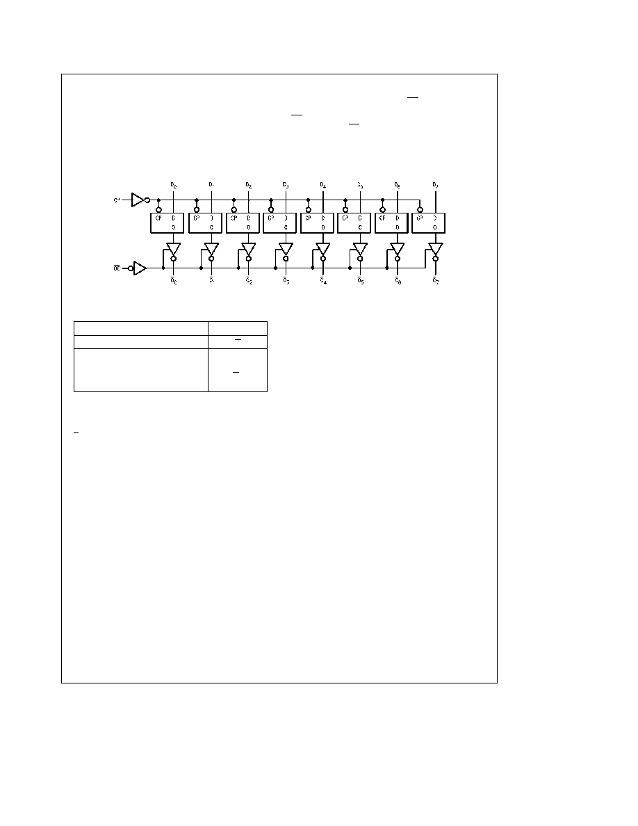
Functional Description
The 'FCT534 consists of eight edge-triggered flip-flops with
individual D-type inputs and TRI-STATE complementary
outputs The buffered clock and buffered Output Enable are
common to all flip-flops The eight flip-flops will store the
state of their individual D inputs that meet the setup and
hold times requirements on the LOW-to-HIGH Clock (CP)
transition With the Output Enable (OE) LOW the contents
of the eight flip-flops are available at the outputs When the
OE is HIGH the outputs go to the high impedance state
Operation of the OE input does not affect the state of the
flip-flops
Logic Diagram
TL F 10665 � 5
Please note that this diagram is provided only for the understanding of logic operations and should not be used to estimate propagation delays
Function Table
Inputs
Output
CP
OE
D
O
L
L
H
L
L
L
L
H
L
L
X
O
0
X
H
X
Z
H
e
HIGH Voltage Level
L
e
LOW Voltage Level
X
e
Immaterial
L
e
LOW-to-HIGH Clock Transition
Z
e
High Impedance
O
0
e
Value stored from previous clock cycle
2
Absolute Maximum Ratings
(Note 1)
If Military Aerospace specified devices are required
please contact the National Semiconductor Sales
Office Distributors for availability and specifications
Terminal Voltage with Respect
to GND (V
TERM
)
74FCT
b
0 5V to
a
7 0V
Temperature Under Bias (T
BIAS
)
74FCT
b
55 C to
a
125 C
Storage Temperature (T
STG
)
74FCT
b
55 C to
a
125 C
DC Output Current (I
OUT
)
120 mA
Note 1
Absolute maximum ratings are those values beyond which damage
to the device may occur Exposure to absolute maximum rating conditions
for extended periods may affect reliability The databook specifications
should be met without exception to ensure that the system design is reli-
able over its power supply temperature and output input loading variables
Recommended Operating
Conditions
Supply Voltage (V
CC
)
74FCT
4 75V to 5 25V
Input Voltage
0V to V
CC
Output Voltage
0V to V
CC
Operating Temperature (T
A
)
74FCT
b
0 C to
a
70 C
Junction Temperature (T
J
)
PDIP
140 C
Note
All commercial packaging is not recommended for applications requir-
ing greater than 2000 temperature cycles from
b
40 C to
a
125 C
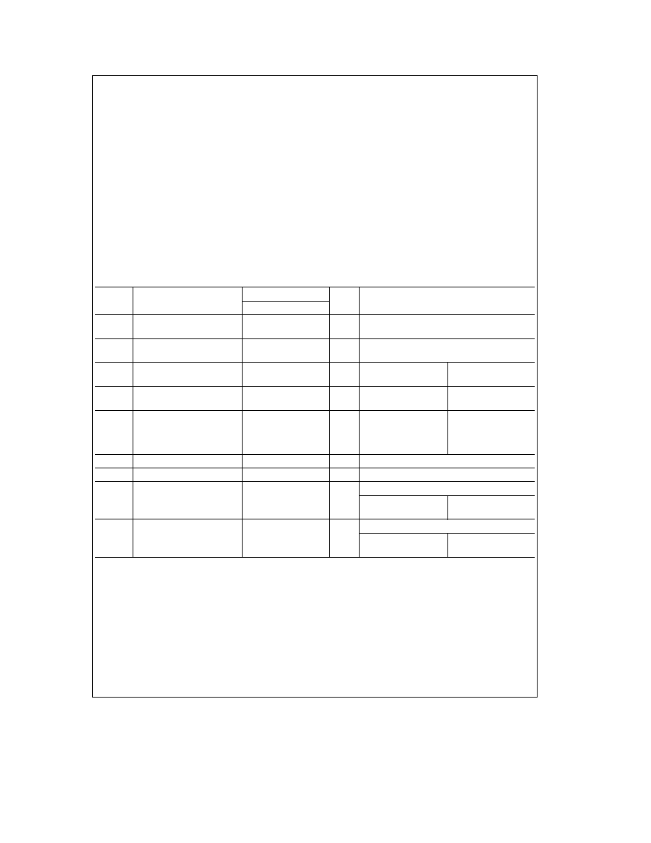
DC Characteristics for 'FCTA Family Devices
Typical values are at V
CC
e
5 0V 25 C ambient and maximum loading For test conditions shown as Max use the value
specified for the appropriate device type Com V
CC
e
5 0V
g
5% T
A
e
0 C to
a
70 C V
HC
e
V
CC
b
0 2V
Symbol
Parameter
74FCTA
Units
Conditions
Min
Typ
Max
V
IH
Minimum High Level
2 0
V
Input Voltage
V
IL
Maximum Low Level
0 8
V
Input Voltage
I
IH
Input High Current
5 0
m
A
V
CC
e
Max
V
I
e
V
CC
5 0
V
I
e
2 7V (Note 2)
I
IL
Input Low Current
b
5 0
m
A
V
CC
e
Max
V
I
e
0 5V (Note 2)
b
5 0
V
I
e
GND
I
OZ
Maximum TRI-STATE Current
2 5
V
CC
e
Max
V
O
e
V
CC
2 5
m
A
V
O
e
2 7V (Note 2)
b
2 5
V
O
e
0 5V (Note 2)
b
2 5
V
O
e
GND
V
IK
Clamp Diode Voltage
b
0 7
b
1 2
V
V
CC
e
Min I
N
e b
18 mA
I
OS
Short Circuit Current
b
60
b
120
mA
V
CC
e
Max (Note 1) V
O
e
GND
V
OH
Minimum High Level
2 8
3 0
V
CC
e
3V V
IN
e
0 2V or V
HC
I
OH
e b
32 mA
Output Voltage
V
HC
V
CC
V
V
CC
e
Min
I
OH
e b
300 mA
2 4
4 3
V
IN
e
V
IH
or V
IL
I
OH
e b
15 mA
V
OL
Maximum Low Level
GND
0 2
V
CC
e
3V V
IN
e
0 2V or V
HC
I
OL
e
300 mA
Output Voltage
GND
0 2
V
V
CC
e
Min
I
OL
e
300 mA
0 3
0 5
V
IN
e
V
IH
or V
IL
I
OL
e
48 mA
3

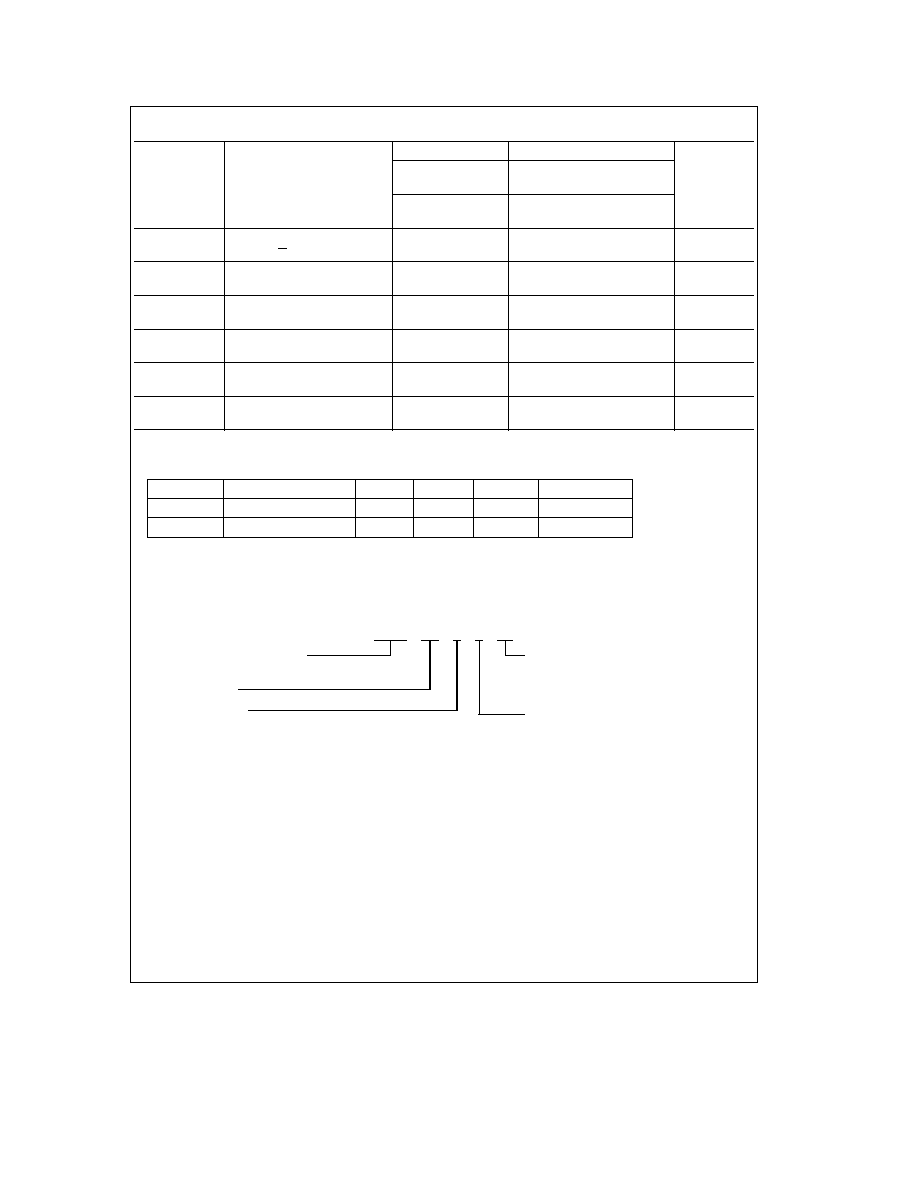
DC Characteristics for 'FCT Family Devices
(Continued)
Typical values are at V
CC
e
5 0V 25 C ambient and maximum loading For test conditions shown as Max use the value
specified for the appropriate device type Com V
CC
e
5 0V
g
5% T
A
e
0 C to
a
70 C V
HC
e
V
CC
b
0 2V
Symbol
Parameter
74FCT
Units
Conditions
Min
Typ
Max
I
CC
Maximum Quiescent
V
CC
e
Max
Supply Current
1 0
40 0
m
A
V
IN
t
V
HC
V
IN
s
0 2V
f
I
e
0
D
I
CC
Quiescent Supply Current
0 5
2 0
mA
V
CC
e
Max
TTL Inputs HIGH
V
IN
e
3 4V (Note 3)
I
CCD
Dynamic Power
V
CC
e
Max
V
IN
t
V
HC
Supply Current (Note 4)
0 15
0 25
mA MHz
Outputs Open
V
IN
s
0 2V
OE
e
GND
One Input Toggling
50% Duty Cycle
I
C
Total Power Supply
V
CC
e
Max
V
IN
t
V
HC
Current (Note 6)
1 5
4 0
Outputs Open
V
IN
s
0 2V
f
CP
e
10 MHz
OE
e
GND
f
I
e
5 MHz
V
IN
e
3 4V
1 8
6 0
One Bit Toggling
V
IN
e
GND
mA
50% Duty Cycle
(Note 5)
V
IN
t
V
HC
V
CC
e
Max
V
IN
s
0 2V
3 0
7 8
Outputs Open
OE
e
GND
f
CP
e
10 MHz
f
I
e
2 5 MHz
V
IN
e
3 4V
5 0
16 8
Eight Bits Toggling
V
IN
e
GND
50% Duty Cycle
V
H
Input Hysteresis
200
mV
on Clock Only
Note 1
Maximum test duration not to exceed one second not more than one output shorted at one time
Note 2
This parameter guaranteed but not tested
Note 3
Per TTL driven input (V
IN
e
3 4V) all other inputs at V
CC
or GND
Note 4
This parameter is not directly testable but is derived for use in Total Power Supply calculations
Note 5
Values for these conditions are examples of the I
CC
formula These limits are guaranteed but not tested
Note 6
I
C
e
I
QUIESCENT
a
I
INPUTS
a
I
DYNAMIC
I
C
e
I
CC
a
D
I
CC
D
H
N
T
a
I
CCD
(f
CP
2
a
f
I
N
I
)
I
CC
e
Quiescent Current
D
I
CC
e
Power Supply Current for a TTL High Input (V
IN
e
3 4V)
D
H
e
Duty Cycle for TTL inputs High
N
T
e
Number of Inputs at D
H
I
CCD
e
Dynamic Current Caused by an Input Transition Pair (HLH or LHL)
f
CP
e
Clock Frequency for Register Devices (Zero for Non-Register Devices)
f
I
e
Input Frequency
N
I
e
Numbers of Inputs at f
I
All currents are in milliamps and all frequencies are in megahertz
4
AC Electrical Characteristics
Symbol
Parameter
74FCT
74FCT
Units
T
A
e a
25 C
T
A
V
CC
e
Com
V
CC
e
5 0V
C
L
e
50 pF
Typ
Min
Max
(Note 1)
t
PLH
Propagation Delay
6 5
1 5
10 0
ns
t
PHL
C
P
to On
t
PZH
Output Enable
9 0
1 5
12 5
ns
t
PZL
Time
t
PHZ
Output Disable
6 0
1 5
8 0
ns
t
PLZ
Time
t
s
Set Up Time High or Low
1 0
2 0
ns
Dn to CP
t
h
Hold Time High or Low
0 5
1 5
ns
Dn to CP
t
w
CP Pulse Width
4 0
7 0
ns
High or Low
Note 1
Minimum limits guaranteed but not tested on propagation delays
Capacitance
T
A
e a
25 C f
I
e
1 0 MHz
Symbol
Parameter
Typ
Max
Units
Conditions
C
IN
Input Capacitance
6
10
pF
V
IN
e
0V
C
OUT
Output Capacitance
8
12
pF
V
OUT
e
0V
Note
This parameter is measured at characterization but not tested
C
OUT
for 74FCT only
Ordering Information
The device number is used to form part of a simplified purchasing code where a package type and temperature range are
defined as follows
74FCT
534
P
C
QR
Temperature Range Family
Special Variations
74FCT
e
Commercial TTL-Compatible
X
e
Devices shipped in 13 reels
QR
e
Commercial grade device
Device Type
with burn-in
Package Code
Temperature Range
P
e
Plastic DIP
C
e
Commercial (0 C to
a
70 C)
S
e
Small Outline (SOIC)
5

6

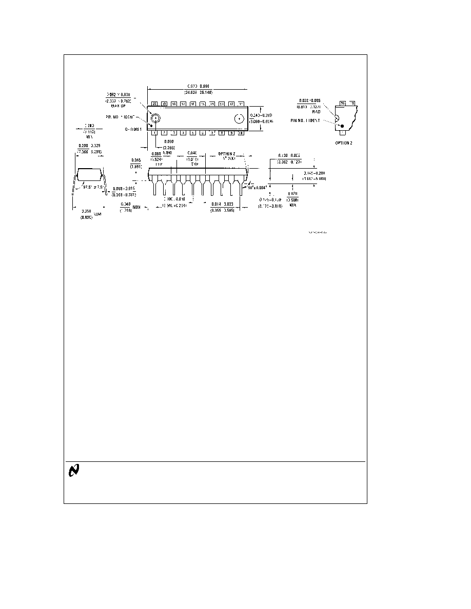
Physical Dimensions
inches (millimeters)
20-Lead Small Outline Integrated Circuit (S)
NS Package Number M20B
7
74FCT534
Octal
D
Flip-Flop
with
TRI-STATE
Outputs
Physical Dimensions
inches (millimeters) (Continued)
20-Lead Plastic Dual-In-Line Package (P)
NS Package Number N20B
LIFE SUPPORT POLICY
NATIONAL'S PRODUCTS ARE NOT AUTHORIZED FOR USE AS CRITICAL COMPONENTS IN LIFE SUPPORT
DEVICES OR SYSTEMS WITHOUT THE EXPRESS WRITTEN APPROVAL OF THE PRESIDENT OF NATIONAL
SEMICONDUCTOR CORPORATION As used herein
1 Life support devices or systems are devices or
2 A critical component is any component of a life
systems which (a) are intended for surgical implant
support device or system whose failure to perform can
into the body or (b) support or sustain life and whose
be reasonably expected to cause the failure of the life
failure to perform when properly used in accordance
support device or system or to affect its safety or
with instructions for use provided in the labeling can
effectiveness
be reasonably expected to result in a significant injury
to the user
National Semiconductor
National Semiconductor
National Semiconductor
National Semiconductor
Corporation
Europe
Hong Kong Ltd
Japan Ltd
1111 West Bardin Road
Fax (a49) 0-180-530 85 86
13th Floor Straight Block
Tel 81-043-299-2309
Arlington TX 76017
Email cnjwge tevm2 nsc com
Ocean Centre 5 Canton Rd
Fax 81-043-299-2408
Tel 1(800) 272-9959
Deutsch Tel (a49) 0-180-530 85 85
Tsimshatsui Kowloon
Fax 1(800) 737-7018
English
Tel (a49) 0-180-532 78 32
Hong Kong
Fran ais Tel (a49) 0-180-532 93 58
Tel (852) 2737-1600
Italiano
Tel (a49) 0-180-534 16 80
Fax (852) 2736-9960
National does not assume any responsibility for use of any circuitry described no circuit patent licenses are implied and National reserves the right at any time without notice to change said circuitry and specifications