 | –≠–ª–µ–∫—Ç—Ä–æ–Ω–Ω—ã–π –∫–æ–º–ø–æ–Ω–µ–Ω—Ç: 74LS168 | –°–∫–∞—á–∞—Ç—å:  PDF PDF  ZIP ZIP |
TL F 10207
54LS168
Synchronous
Bi-Directional
BCD
Decade
Counter
June 1989
54LS168 Synchronous Bi-Directional
BCD Decade Counter
General Description
The 54LS168 is a fully synchronous 4-state up down coun-
ter featuring a preset capability for programmable operation
carry lookahead for easy cascading and a U D input to con-
trol the direction of counting It counts in the BCD (8421)
sequence and all state changes whether in counting or par-
allel loading are initiated by the LOW-to-HIGH transition of
the clock
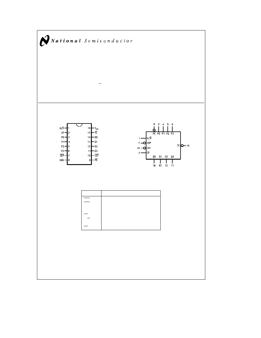
Connection Diagram
Dual-In-Line Package
TL F 10207 ≠ 1
Order Number 54LS168DMQB
54LS168FMQB or 54LS168LMQB
See NS Package Number
E20A J16A or W16A
Logic Symbol
TL F 10207 ≠ 2
V
CC
e
Pin 16
GND
e
Pin 8
Pin Names
Description
CEP
Count Enable Parallel Input (Active LOW)
CET
Count Enable Trickle Input (Active LOW)
CP
Clock Pulse Input (Active Rising Edge)
P0 ≠ P3
Parallel Data Inputs
PE
Parallel Enable Input (Active LOW)
U D
Up-Down Count Control Input
Q0 ≠ Q3
Flip-Flop Outputs
TC
Terminal Count Output (Active LOW)
C1995 National Semiconductor Corporation
RRD-B30M105 Printed in U S A
Absolute Maximum Ratings
(Note)
If Military Aerospace specified devices are required
please contact the National Semiconductor Sales
Office Distributors for availability and specifications
Supply Voltage
7V
Input Voltage
5 5V
Operating Free Air Temperature Range
54LS
b
55 C to
a
125 C
Storage Temperature Range
b
65 C to
a
150 C
Note
The ``Absolute Maximum Ratings'' are those values
beyond which the safety of the device cannot be guaran-
teed The device should not be operated at these limits The
parametric values defined in the ``Electrical Characteristics''
table are not guaranteed at the absolute maximum ratings
The ``Recommended Operating Conditions'' table will define
the conditions for actual device operation
Recommended Operating Conditions
Symbol
Parameter
54LS168
Units
Min
Nom
Max
V
CC
Supply Voltage
4 5
5
5 5
V
V
IH
High Level Input Voltage
2
V
V
IL
Low Level Input Voltage
0 7
V
I
OH
High Level Output Current
b
0 4
mA
I
OL
Low Level Output Current
4
mA
T
A
Free Air Operating Temperature
b
55
125
C
t
s
(H)
Setup Time HIGH or LOW
15
ns
t
s
(L)
P
n
CEP or CET to CP
15
t
h
(H)
Hold Time HIGH or LOW
5
ns
t
h
(L)
P
n
CEP or CET to CP
5
t
s
(H)
Setup Time HIGH or LOW
20
ns
t
s
(L)
PE to CP
20
t
h
(H)
Hold Time HIGH or LOW
0
ns
t
h
(L)
PE to CP
0
t
s
(H)
Setup Time HIGH or LOW
25
ns
t
s
(L)
U D to CP
25
t
h
(H)
Hold Time HIGH or LOW
0
ns
t
h
(L)
U D to CP
0
t
w
(H)
CP Pulse Width HIGH or LOW
20
ns
t
w
(L)
20
2
Electrical Characteristics
over recommended operating free air temperature range (unless otherwise noted)
Symbol
Parameter
Conditions
Min
Typ
Max
Units
(Note 1)
V
I
Input Clamp Voltage
V
CC
e
Min I
I
e b
18 mA
b
1 5
V
V
OH
High Level Output Voltage
V
CC
e
Min I
OH
e
Max
2 5
V
V
IL
e
Max V
IH
e
Min
V
OL
Low Level Output Voltage
V
CC
e
Min I
OL
e
Max
0 4
V
V
IH
e
Min V
IL
e
Max
I
I
Input Current
Max
V
CC
e
Max V
I
e
10 0V
0 1
mA
Input Voltage
I
IH
High Level Input Current
V
CC
e
Max V
I
e
2 7V
Inputs
20
m
A
CET
40
I
IL
Low Level Input Current
V
CC
e
Max V
I
e
0 5V
Data
b
0 5
b
400
CP PE U D CEP
b
30
b
400
m
A
CET
b
60
b
800
I
OS
Short Circuit Output Current
V
CC
e
Max (Note 2)
b
20
b
100
mA
I
CC
Supply Current
V
CC
e
Max (Note 3)
34
mA
Note 1
All typicals are at V
CC
e
5V T
A
e
25 C
Note 2
Not more than one output should be shorted at a time and the duration should not exceed one second
Note 3
I
CC
is measured with all outputs open and all inputs grounded
Switching Characteristics
V
CC
e a
5 0V T
A
e a
25 C (See Section 1 for test waveforms and output load)
54LS168
Symbol
Parameter
C
L
e
15 pF
Units
Min
Max
f
Max
Maximum Clock Frequency
25
MHz
t
PLH
Propagation Delay
20
ns
t
PHL
CP to Q
n
20
t
PLH
Propagation Delay
30
ns
t
PHL
CP to TC
30
t
PLH
Propagation Delay
15
ns
t
PHL
CET to TC
20
t
PLH
Propagation Delay
25
ns
t
PHL
U D to TC
25
3
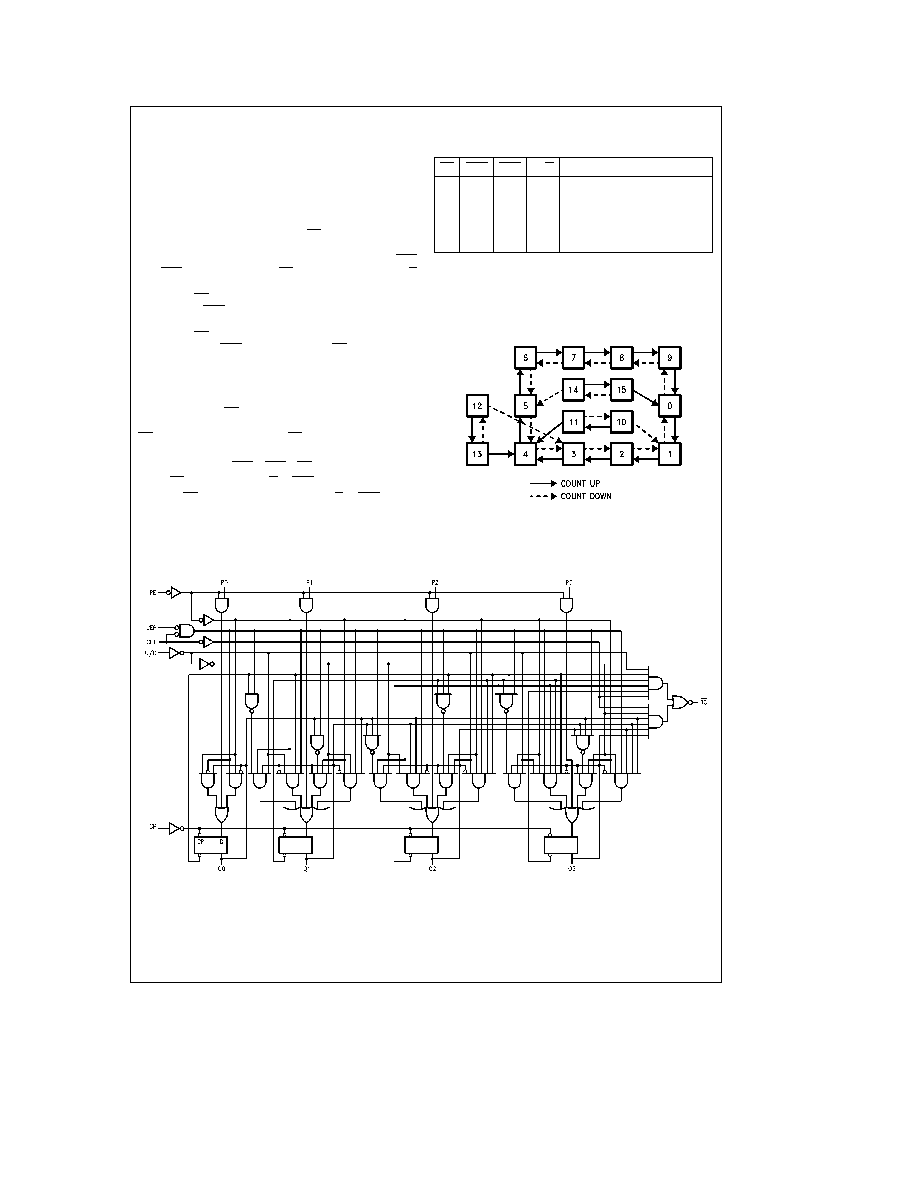
Functional Description
The 'LS168 uses edge-triggered D-type flip-flops and has
no constraints on changing the control or data input signals
in either state of the Clock The only requirement is that the
various inputs attain the desired state at least a setup time
before the rising edge of the clock and remain valid for the
recommended hold time thereafter The parallel load opera-
tion takes precedence over the other operations as indicat-
ed in the Mode Select Table When PE is LOW the data on
the P0 ≠ P3 inputs enters the flip-flops on the next rising
edge of the Clock In order for counting to occur both CEP
and CET must be LOW and PE must be HIGH The U D
input then determines the direction of counting The Termi-
nal Count (TC) output is normally HIGH and goes LOW
provided that CET is LOW when a counter reaches zero in
the COUNT DOWN mode or reaches 9 in the COUNT UP
mode The TC output state is not a function of the Count
Enable Parallel (CEP) input level The TC output of the
'LS168 decade counter can also be LOW in the illegal
states 11 13 and 15 which can occur when power is turned
on or via parallel loading If an illegal state occurs the
'LS168 will return to the legitimate sequence within two
counts Since the TC signal is derived by decoding the flip-
flop states there exists the possibility of decoding spikes on
TC For this reason the use of TC as a clock signal is not
recommended (see logic equation below)
1 Count Enable
e
CEP
CET
PE
2 Up TC
e
Q0
Q3
(U D)
CET
3 Down TC
e
Q0
Q1
Q2
Q3
(U D)
CET
'LS168 Mode Select Table
PE
CEP
CET
U D
Action on Rising Clock Edge
L
X
X
X
Load (P
n
x
Q
n
)
H
L
L
H
Count Up (Increment)
H
L
L
L
Count Down (Decrement)
H
H
X
X
No Change (Hold)
H
X
H
X
No Change (Hold)
H
e
HIGH Voltage Level
L
e
LOW Voltage Level
X
e
Immaterial
State Diagram
TL F 10207 ≠ 3
Logic Diagram
TL F 10207 ≠ 4
4
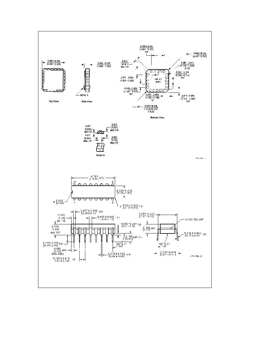
Physical Dimensions
inches (millimeters)
Ceramic Leadless Chip Carrier Package (E)
Order Number 54LS168LMQB
NS Package Number E20A
16-Lead Ceramic Dual-In-Line Package (J)
Order Number 54LS168DMQB
NS Package Number J16A
5