TL F 6431
DM54LS373DM74LS373
DM54LS374DM74LS374
TRI-STATE
Octal
D-Type
Transparent
Latches
and
Edge-Triggered
Flip-Flops
May 1992
DM54LS373 DM74LS373
DM54LS374 DM74LS374
TRI-STATE
Octal D-Type Transparent
Latches and Edge-Triggered Flip-Flops
General Description
These 8-bit registers feature totem-pole TRI-STATE outputs
designed specifically for driving highly-capacitive or relative-
ly low-impedance loads The high-impedance state and in-
creased high-logic level drive provide these registers with
the capability of being connected directly to and driving the
bus lines in a bus-organized system without need for inter-
face or pull-up components They are particularly attractive
for implementing buffer registers I O ports bidirectional
bus drivers and working registers
(Continued)
Features
Y
Choice of 8 latches or 8 D-type flip-flops in a single
package
Y
TRI-STATE bus-driving outputs
Y
Full parallel-access for loading
Y
Buffered control inputs
Y
P-N-P inputs reduce D-C loading on data lines
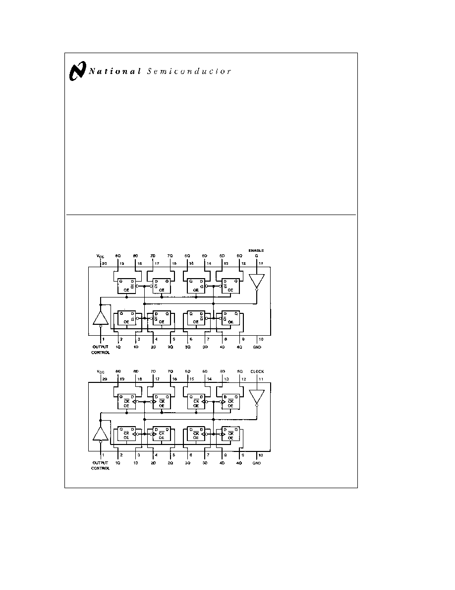
Connection Diagrams
Dual-In-Line Packages
'LS373
TL F 6431 � 1
Order Number
DM54LS373J
DM54LS373W
DM74LS373N or
DM74LS373WM
See NS Package Number
J20A M20B N20A or
W20A
'LS374
TL F 6431 � 2
Order Number
DM54LS374J
DM54LS374W
DM74LS374WM or
DM74LS374N
See NS Package Number
J20A M20B N20A or
W20A
TRI-STATE
is a registered trademark of National Semiconductor Corp
C1995 National Semiconductor Corporation
RRD-B30M105 Printed in U S A
General Description
(Continued)
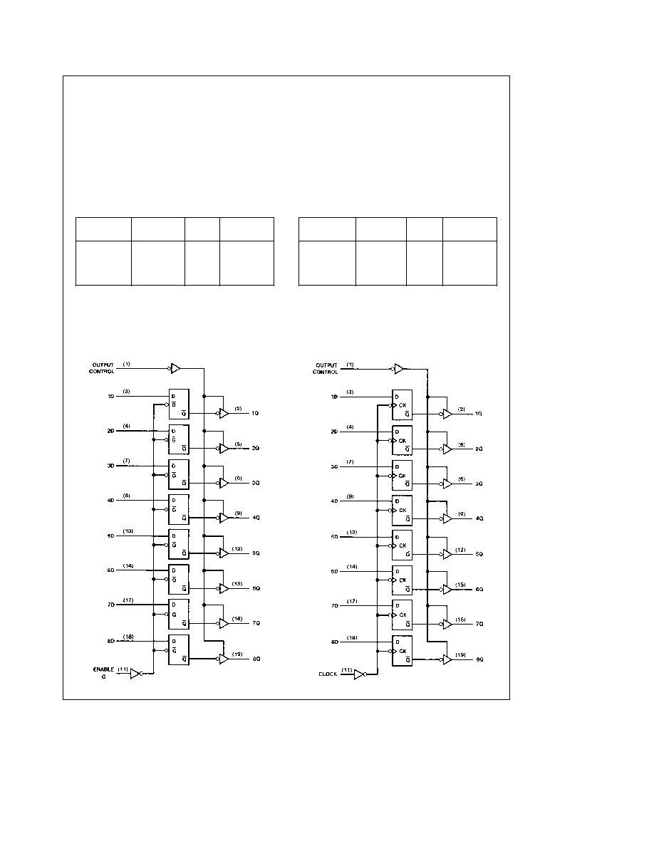
The eight latches of the DM54 74LS373 are transparent D-
type latches meaning that while the enable (G) is high the Q
outputs will follow the data (D) inputs When the enable is
taken low the output will be latched at the level of the data
that was set up
The eight flip-flops of the DM54 74LS374 are edge-trig-
gered D-type flip flops On the positive transition of the
clock the Q outputs will be set to the logic states that were
set up at the D inputs
A buffered output control input can be used to place the
eight outputs in either a normal logic state (high or low logic
levels) or a high-impedance state In the high-impedance
state the outputs neither load nor drive the bus lines signifi-
cantly
The output control does not affect the internal operation of
the latches or flip-flops That is the old data can be retained
or new data can be entered even while the outputs are off
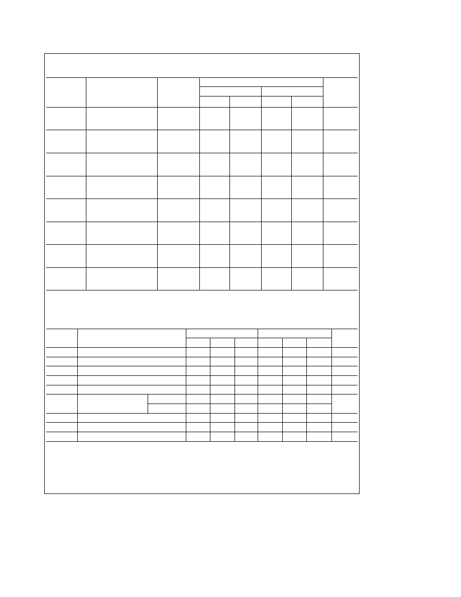
Function Tables
DM54 74LS373
Output
Enable
D
Output
Control
G
L
H
H
H
L
H
L
L
L
L
X
Q
0
H
X
X
Z
DM54 74LS374
Output
Clock
D
Output
Control
L
u
H
H
L
u
L
L
L
L
X
Q
0
H
X
X
Z
H
e
High Level (Steady State) L
e
Low Level (Steady State) X
e
Don't Care
u
e
Transition from low-to-high level Z
e
High Impedance State
Q
0
e
The level of the output before steady-state input conditions were established
Logic Diagrams
DM54 74LS373
Transparent Latches
TL F 6431 � 3
DM54 74LS374
Positive-Edge-Triggered Flip-Flops
TL F 6431 � 4
2

Absolute Maximum Ratings
(See Note)
If Military Aerospace specified devices are required
please contact the National Semiconductor Sales
Office Distributors for availability and specifications
Supply Voltage
7V
Input Voltage
7V
Storage Temperature Range
b
65 C to
a
150 C
Operating Free Air Temperature Range
DM54LS
b
55 C to
a
125 C
DM74LS
0 C to
a
70 C
Note
The ``Absolute Maximum Ratings'' are those values
beyond which the safety of the device cannot be guaran-
teed The device should not be operated at these limits The
parametric values defined in the ``Electrical Characteristics''
table are not guaranteed at the absolute maximum ratings
The ``Recommended Operating Conditions'' table will define
the conditions for actual device operation
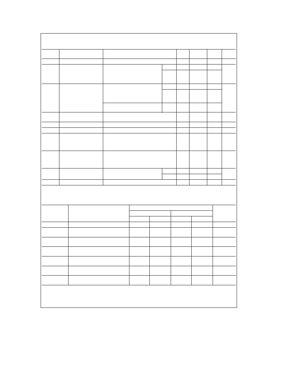
Recommended Operating Conditions
Symbol
Parameter
DM54LS373
DM74LS373
Units
Min
Nom
Max
Min
Nom
Max
V
CC
Supply Voltage
4 5
5
5 5
4 75
5
5 25
V
V
IH
High Level Input Votage
2
2
V
V
IL
Low Level Input Voltage
0 7
0 8
V
I
OH
High Level Output Current
b
1
b
2 6
mA
I
OL
Low Level Output Current
12
24
mA
t
W
Pulse Width
Enable High
15
15
ns
(Note 2)
Enable Low
15
15
t
SU
Data Setup Time (Notes 1
2)
5
v
5
v
ns
t
H
Data Hold Time (Notes 1
2)
20
v
20
v
ns
T
A
Free Air Operating Temperature
b
55
125
0
70
C
Note 1
The symbol (
v
) indicates the falling edge of the clock pulse is used for reference
Note 2
T
A
e
25 C and V
CC
e
5V
'LS373 Electrical Characteristics
over recommended operating free air temperature range (unless otherwise noted)
Symbol
Parameter
Conditions
Min
Typ
Max
Units
(Note 1)
V
I
Input Clamp Voltage
V
CC
e
Min I
I
e b
18 mA
b
1 5
V
V
OH
High Level Output Voltage
V
CC
e
Min
DM54
2 4
3 4
I
OH
e
Max
V
V
IL
e
Max
DM74
2 4
3 1
V
IH
e
Min
V
OL
Low Level Output Voltage
V
CC
e
Min
DM54
0 25
0 4
I
OL
e
Max
V
IL
e
Max
DM74
0 35
0 5
V
V
IH
e
Min
I
OL
e
12 mA
DM74
0 4
V
CC
e
Min
I
I
Input Current
Max
V
CC
e
Max V
I
e
7V
0 1
mA
Input Voltage
I
IH
High Level Input Current
V
CC
e
Max V
I
e
2 7V
20
m
A
I
IL
Low Level Input Current
V
CC
e
Max V
I
e
0 4V
b
0 4
mA
I
OZH
Off-State Output Current
V
CC
e
Max V
O
e
2 7V
with High Level Output
V
IH
e
Min V
IL
e
Max
20
m
A
Voltage Applied
I
OZL
Off-State Output Current
V
CC
e
Max V
O
e
0 4V
with Low Level Output
V
IH
e
Min V
IL
e
Max
b
20
m
A
Voltage Applied
I
OS
Short Circuit
V
CC
e
Max
DM54
b
20
b
100
mA
Output Current
(Note 2)
DM74
b
50
b
225
I
CC
Supply Current
V
CC
e
Max OC
e
4 5V
24
40
mA
D
n
Enable
e
GND
3
`LS373 Switching Characteristics
at V
CC
e
5V and T
A
e
25 C
(See Section 1 for Test Waveforms and Output Load)
From
R
L
e
667X
(Input)
Symbol
Parameter
C
L
e
45 pF
C
L
e
150 pF
Units
To
Min
Max
Min
Max
(Output)
t
PLH
Propagation Delay
Data
Time Low to High
to
18
26
ns
Level Output
Q
t
PHL
Propagation Delay
Data
Time High to Low
to
18
27
ns
Level Output
Q
t
PLH
Propagation Delay
Enable
Time Low to High
to
30
38
ns
Level Output
Q
t
PHL
Propagation Delay
Enable
Time High to Low
to
30
36
ns
Level Output
Q
t
PZH
Output Enable
Output
Time to High
Control
28
36
ns
Level Output
to Any Q
t
PZL
Output Enable
Output
Time to Low
Control
36
50
ns
Level Output
to Any Q
t
PHZ
Output Disable
Output
Time from High
Control
20
ns
Level Output (Note 3)
to Any Q
t
PLZ
Output Disable
Output
Time from Low
Control
25
ns
Level Output (Note 3)
to Any Q
Note 1
All typicals are at V
CC
e
5V T
A
e
25 C
Note 2
Not more than one output should be shorted at a time and the duration should not exceed one second
Note 3
C
L
e
5 pF
Recommended Operating Conditions
Symbol
Parameter
DM54LS374
DM74LS374
Units
Min
Nom
Max
Min
Nom
Max
V
CC
Supply Voltage
4 5
5
5 5
4 75
5
5 25
V
V
IH
High Level Input Voltage
2
2
V
V
IL
Low Level Input Voltage
0 7
0 8
V
I
OH
High Level Output Current
b
1
b
2 6
mA
I
OL
Low Level Output Current
12
24
mA
t
W
Pulse Width
Clock High
15
15
ns
(Note 4)
Clock Low
15
15
t
SU
Data Setup Time (Notes 1
4)
20
u
20
u
ns
t
H
Data Hold Time (Notes 1
4)
1
u
1
u
ns
T
A
Free Air Operating Temperature
b
55
125
0
70
C
Note 1
The symbol (
u
) indicates the rising edge of the clock pulse is used for reference
Note 4
T
A
e
25 C and V
CC
e
5V
4
'LS374 Electrical Characteristics
over recommended operating free air temperature range (unless otherwise noted)
Symbol
Parameter
Conditions
Min
Typ
Max
Units
(Note 1)
V
I
Input Clamp Voltage
V
CC
e
Min I
I
e b
18 mA
b
1 5
V
V
OH
High Level Output Voltage
V
CC
e
Min
DM54
2 4
3 4
I
OH
e
Max
DM74
2 4
3 1
V
V
IL
e
Max
V
IH
e
Min
V
OL
Low Level Output Voltage
V
CC
e
Min
DM54
0 25
0 4
I
OL
e
Max
DM74
0 35
0 5
V
IL
e
Max
V
V
IH
e
Min
I
OL
e
12 mA
DM74
0 25
0 4
V
CC
e
Min
I
I
Input Current
Max
V
CC
e
Max V
I
e
7V
0 1
mA
Input Voltage
I
IH
High Level Input Current
V
CC
e
Max V
I
e
2 7V
20
m
A
I
IL
Low Level Input Current
V
CC
e
Max V
I
e
0 4V
b
0 4
mA
I
OZH
Off-State Output
V
CC
e
Max V
O
e
2 7V
Current with High
V
IH
e
Min V
IL
e
Max
20
m
A
Level Output
Voltage Applied
I
OZL
Off-State Output
V
CC
e
Max V
O
e
0 4V
Current with Low
V
IH
e
Min V
IL
e
Max
b
20
m
A
Level Output
Voltage Applied
I
OS
Short Circuit
V
CC
e
Max
DM54
b
50
b
225
mA
Output Current
(Note 2)
DM74
b
50
b
225
I
CC
Supply Current
V
CC
e
Max D
n
e
GND OC
e
4 5V
27
45
mA
'LS374 Switching Characteristics
at V
CC
e
5V and T
A
e
25 C
(See Section 1 for Test Waveforms and Output Load)
R
L
e
667X
Symbol
Parameter
C
L
e
45 pF
C
L
e
150 pF
Units
Min
Max
Min
Max
f
MAX
Maximum Clock Frequency
35
20
MHz
t
PLH
Propagation Delay Time
28
32
ns
Low to High Level Output
t
PHL
Propagation Delay Time
28
38
ns
High to Low Level Output
t
PZH
Output Enable Time
28
44
ns
to High Level Output
t
PZL
Output Enable Time
28
44
ns
to Low Level Output
t
PHZ
Output Disable Time
20
ns
from High Level Output (Note 3)
t
PLZ
Output Disable Time
25
ns
from Low Level Output (Note 3)
Note 1
All typicals are at V
CC
e
5V T
A
e
25 C
Note 2
Not more than one output should be shorted at a time and the duration should not exceed one second
Note 3
C
L
e
5 pF
5