 | –≠–ª–µ–∫—Ç—Ä–æ–Ω–Ω—ã–π –∫–æ–º–ø–æ–Ω–µ–Ω—Ç: 74LS48 | –°–∫–∞—á–∞—Ç—å:  PDF PDF  ZIP ZIP |
TL F 10172
DM74LS48
BCD
to
7-Segment
Decoder
January 1992
DM74LS48
BCD to 7-Segment Decoder
General Description
The 'LS48 translates four lines of BCD (8421) input data
into the 7-segment numeral code and provides seven corre-
sponding outputs having pull-up resistors as opposed to
totem pole pull-ups These outputs can serve as logic sig-
nals with a HIGH output corresponding to a lighted lamp
segment or can provide a 1 3 mA base current to npn lamp
driver transistors Auxiliary inputs provide lamp test blank-
ing and cascadable zero-suppression functions
The 'LS48 decodes the input data in the pattern indicated in
the Truth Table and the segment identification illustration
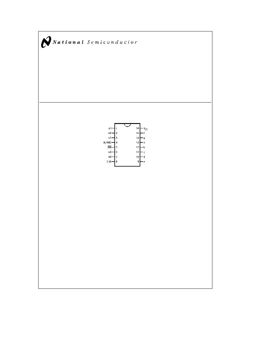
Connection Diagram
Dual-In-Line Package
TL F 10172 ≠ 1
Order Number DM74LS48M or DM74LS48N
See NS Package Number M16A or N16E
C1995 National Semiconductor Corporation
RRD-B30M105 Printed in U S A
Absolute Maximum Ratings
(Note)
Supply Voltage
7V
Input Voltage
7V
Operating Free Air Temperature Range
DM74LS
0 C to
a
70 C
Storage Temperature Range
b
65 C to
a
150 C
Note
The ``Absolute Maximum Ratings'' are those values
beyond which the safety of the device cannot be guaran-
teed The device should not be operated at these limits The
parametric values defined in the ``Electrical Characteristics''
table are not guaranteed at the absolute maximum ratings
The ``Recommended Operating Conditions'' table will define
the conditions for actual device operation
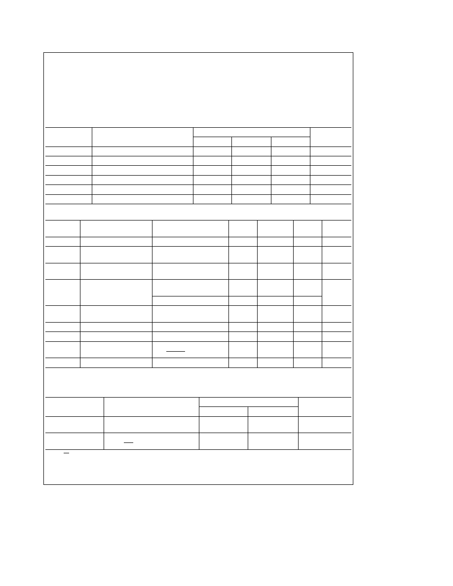
Recommended Operating Conditions
Symbol
Parameter
DM74LS48
Units
Min
Nom
Max
V
CC
Supply Voltage
4 75
5
5 25
V
V
IH
High Level Input Voltage
2
V
V
IL
Low Level Input Voltage
0 8
V
I
OH
High Level Output Current
b
50
m
A
I
OL
Low Level Output Current
6 0
mA
T
A
Free Air Operating Temperature
0
70
C
Electrical Characteristics
over recommended operating free air temperature range (unless otherwise noted)
Symbol
Parameter
Conditions
Min
Typ
Max
Units
(Note 1)
V
I
Input Clamp Voltage
V
CC
e
Min I
I
e b
18 mA
b
1 5
V
V
OH
High Level Output
V
CC
Min I
OH
e
Max
2 4
V
Voltage
V
IL
e
Max
I
OFF
Output High Current
V
CC
e
Min V
O
e
0 85V
b
1 3
mA
Segment Outputs
V
OL
Low Level Output
V
CC
e
Min I
OL
e
Max
0 5
Voltage
V
IH
e
Min
V
I
OL
e
2 0 mA V
CC
e
Min
0 4
I
I
Input Current
Max
V
CC
e
Max V
I
e
7V
0 1
mA
Input Voltage
I
IH
High Level Input Current
V
CC
e
Max V
I
e
2 7V
20
m
A
I
IL
Low Level Input Current
V
CC
e
Max V
I
e
0 4V
b
0 4
mA
I
OS
Short Circuit
V
CC
e
Max V
O
e
0V
b
0 3
b
2
mA
Output Current
at BI RBO (Note 2)
I
CCH
Supply Current
V
CC
e
Max V
IN
e
4 5V
38
mA
Note 1
All typicals are at V
CC
e
5V T
A
e
25 C
Note 2
Not more than one output should be shorted at a time and the duration should not exceed one second
Switching Characteristics
at V
CC
e
5V and T
A
e
25 C
Symbol
Parameter
C
L
e
15 pF
Units
Min
Max
t
PLH
Propagation Delay Time
100
ns
t
PHL
A
n
to a ≠ g
100
t
PLH
Propagation Delay Time
100
ns
t
PHL
RBI to a ≠ f
100
Note
LT
e
HIGH A
0
≠A
3
e
HIGH
2
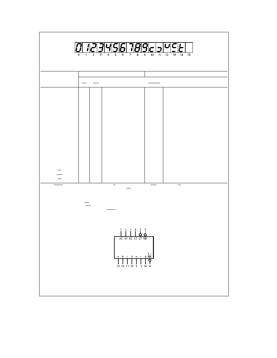
Numerical Designations
Resultant Displays
TL F 10172 ≠ 4
Truth Table
Decimal
Inputs
Outputs
Or
Function
LT
RBI
A
3
A
2
A
1
A
0
BI RBO
a
b
c
d
e
f
g
0 (Note 1)
H
H
L
L
L
L
H
H
H
H
H
H
H
L
1 (Note 1)
H
X
L
L
L
H
H
L
H
H
L
L
L
L
2
H
X
L
L
H
L
H
H
H
L
H
H
L
H
3
H
X
L
L
H
H
H
H
H
H
H
L
L
H
4
H
X
L
H
L
L
H
L
H
H
L
L
H
H
5
H
X
L
H
L
H
H
H
L
H
H
L
H
H
6
H
X
L
H
H
L
H
L
L
H
H
H
H
H
7
H
X
L
H
H
H
H
H
H
H
L
L
L
L
8
H
X
H
L
L
L
H
H
H
H
H
H
H
H
9
H
X
H
L
L
H
H
H
H
H
L
L
H
H
10
H
X
H
L
H
L
H
L
L
L
H
H
L
H
11
H
X
H
L
H
H
H
L
L
H
H
L
L
H
12
H
X
H
H
L
L
H
L
H
L
L
L
H
H
13
H
X
H
H
L
H
H
H
L
L
H
L
H
H
14
H
X
H
H
H
L
H
L
L
L
H
H
H
H
15
H
X
H
H
H
H
H
L
L
L
L
L
L
L
BI (Note 2)
X
X
X
X
X
X
L
L
L
L
L
L
L
L
RBI (Note 3)
H
L
L
L
L
L
L
L
L
L
L
L
L
L
LT (Note 4)
L
X
X
X
X
X
H
H
H
H
H
H
H
H
Note 1
BI RBO is wired-AND logic serving as blanking input (BI) and or ripple-blanking output (RBO) The blanking out (BI) must be open or held at a HIGH level
when output functions 0 through 15 are desired and ripple-blanking input (RBI) must be open or at a HIGH level if blanking of a decimal 0 is not desired X
e
input
may be HIGH or LOW
Note 2
When a LOW level is applied to the blanking input (forced condition) all segment outputs go to a LOW level regardless of the state of any other input
condition
Note 3
When ripple-blanking input (RBI) and inputs A
0
A
1
A
2
and A
3
are at LOW level with the lamp test input at HIGH level all segment outputs go to a LOW
level and the ripple-blanking output (RBO) goes to a LOW level (response condition)
Note 4
When the blanking input ripple-blanking output (BI RBO) is open or held at a HIGH level and a LOW level is applied to lamp test input all segment outputs
go to a HIGH level
Logic Symbol
TL F 10172 ≠ 2
V
CC
e
Pin 16
GND
e
Pin 8
3

Logic Diagram
TL F 10172 ≠ 3
4
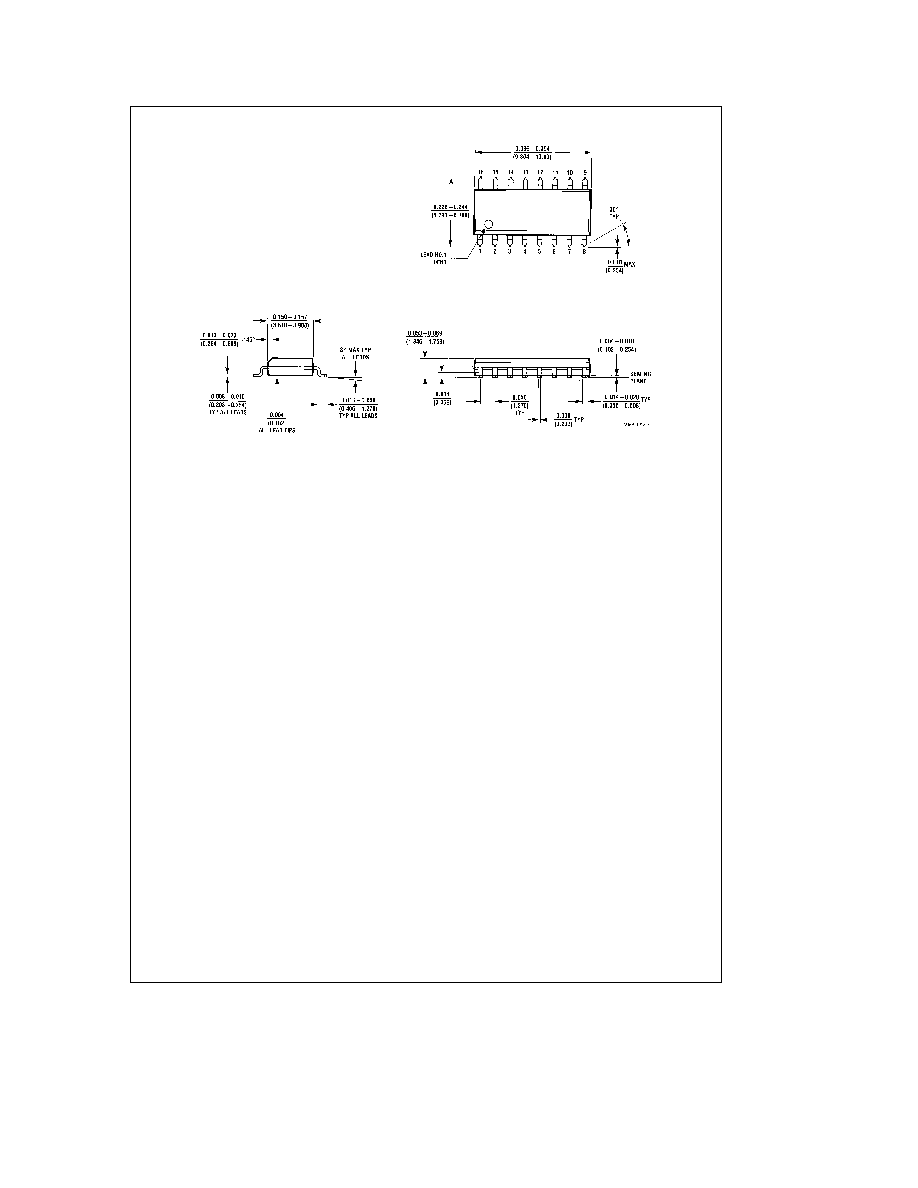
Physical Dimensions
inches (millimeters)
16-Lead Small Outline Molded Package (M)
Order Number DM74LS48M
NS Package Number M16A
5