TL F 12024
74LVT16652
33V
ABT
16-Bit
TransceiverRegister
with
TRI-STATE
Outputs
ADVANCE INFORMATION
October 1995
74LVT16652
3 3V ABT 16-Bit Transceiver Register
with TRI-STATE
Outputs
General Description
The LVT16652 consists of sixteen bus transceiver circuits
with D-type flip-flops and control circuitry arranged for multi-
plexed transmission of data directly from the input bus or
from the internal registers Each byte has separate control
inputs which can be shorted together for full 16-bit opera-
tion Data on the A or B bus will be clocked into the registers
as the appropriate clock pin goes to HIGH logic level Out-
put Enable pins (OEAB OEBA) are provided to control the
transceiver function
The transceivers are designed for low-voltage (3 3V) V
CC
applications but with the capability to provide a TTL inter-
face to a 5V environment The LVT16652 is fabricated with
an advanced BiCMOS technology to achieve high speed
operation similar to 5V ABT while maintaining a low power
dissipation
Features
Y
Input and output interface capability to systems at 5V
V
CC
Y
Bus-Hold data inputs eliminate the need for external
pull-up resistors to hold unused inputs
Y
Live insertion extraction permitted
Y
Power Up Down high impedance provides glitch-free
bus loading
Y
Outputs source sink
b
32 mA
a
64 mA
Y
Available in SSOP and TSSOP
Y
Functionally compatible with the 74 series 16652
Y
Latch-up performance exceeds 500 mA
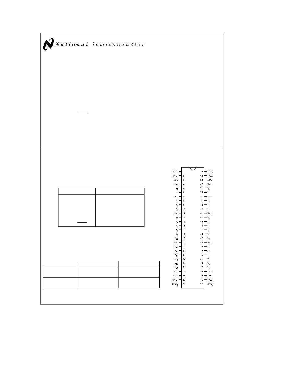
Pin Names
Description
A
0
≠ A
16
Data Register A Inputs
TRI-STATE Outputs
B
0
≠ B
16
Data Register B Inputs
TRI-STATE Outputs
CPAB
n
CPBA
n
Clock Pulse Inputs
SAB
n
SBA
n
Select Inputs
OEAB
n
OEBA
n
Output Enable Inputs
SSOP EIAJ
TSSOP JEDEC
Order Number
74LVT16652MEA
74LVT16652MTD
74LVT16652MEAX
74LVT16652MTDX
NS Package
MS56A
MTD56
Number
Connection Diagram
Pin Assignment for
SSOP and TSSOP
TL F 12024 ≠ 1
TRI-STATE
is a registered trademark of National Semiconductor Corporation
C1996 National Semiconductor Corporation
RRD-B30M17 Printed in U S A
http
www national com

Functional Description
In the transceiver mode data present at the HIGH imped-
ance port may be stored in either the A or B register or both
The select (SAB
n
SBA
n
) controls can multiplex stored and
real-time
The examples in
Figure 1 demonstrate the four fundamental
bus-management functions that can be performed with the
LVT16652
Data on the A or B data bus or both can be stored in the
internal D flip-flop by LOW to HIGH transitions at the appro-
priate Clock Inputs (CPAB
n
CPBA
n
) regardless of the Se-
lect or Output Enable Inputs When SAB and SBA are in the
real time transfer mode it is also possible to store data
without using the internal D flip-flops by simultaneously en-
abling OEAB
n
and OEBA
n
In this configuration each Output
reinforces its Input Thus when all other data sources to the
two sets of bus lines are in a HIGH impedance state each
set of bus lines will remain at its last state
Real-Time Transfer
Bus B to Bus A
TL F 12024 ≠ 4
OEAB1 OEBA1 CPAB1 CPBA1 SAB1 SBA1
L
L
X
X
X
L
Real-Time Transfer
Bus A to Bus B
TL F 12024 ≠ 5
OEAB1 OEBA1 CPAB1 CPBA1 SAB1 SBA1
H
H
X
X
L
X
Storage
TL F 12024 ≠ 6
OEAB1 OEBA1 CPAB1 CPBA1 SAB1 SBA1
X
H
L
X
X
X
L
X
X
L
X
X
L
H
L
L
X
X
Transfer Storage
Data to A or B
TL F 12024 ≠ 7
OEAB1 OEBA1 CPAB1 CPBA1 SAB1 SBA1
H
L
H or L
H or L
H
H
FIGURE 1
Truth Table
(Note)
Inputs
Inputs Outputs
Operating Mode
OEAB
1
OEBA
1
CPAB
1
CPBA
1
SAB
1
SBA
1
A
0
thru A
7
B
0
thru B
7
L
H
H or L
H or L
X
X
Input
Input
Isolation
L
H
L
L
X
X
Store A and B Data
X
H
L
H or L
X
X
Input
Not Specified
Store A Hold B
H
H
L
L
X
X
Input
Output
Store A in Both Registers
L
X
H or L
L
X
X
Not Specified
Input
Hold A Store B
L
L
L
L
X
X
Output
Input
Store B in Both Registers
L
L
X
X
X
L
Output
Input
Real-Time B Data to A Bus
L
L
X
H or L
X
H
Store B Data to A Bus
H
H
X
X
L
X
Input
Output
Real-Time A Data to B Bus
H
H
H or L
X
H
X
Stored A Data to B Bus
H
L
H or L
H or L
H
H
Output
Output
Stored A Data to B Bus and
Stored B Data to A Bus
H
e
HIGH Voltage Level
L
e
LOW Voltage Level
X
e
Immaterial
L
e
LOW to HIGH Clock Transition
Note
The data output functions may be enabled or disabled by various signals at OEAB or OEBA inputs Data input functions are always enabled i e data at the
bus pins will be stored on every LOW to HIGH transition on the clock inputs This also applies to data I O (A and B 8≠15) and
2 control pins
http
www national com
3

74LVT16652 Ordering Information
The device number is used to form part of a simplified purchasing code where the package type and temperature range are
defined as follows
74LVT
16652
MEA
X
Temperature Range Family
Special Variations
74LVT
e
Commercial
``X''
e
Tape and Reel
`` ''
e
Rail Tube
Device Type
Package Code
MEA
e
Molded Shrink Small Outline Package EIAJ
MTD
e
Molded Thin Shrink Small Outline Package JEDEC 4 4 mm
Body Width
http
www national com
4
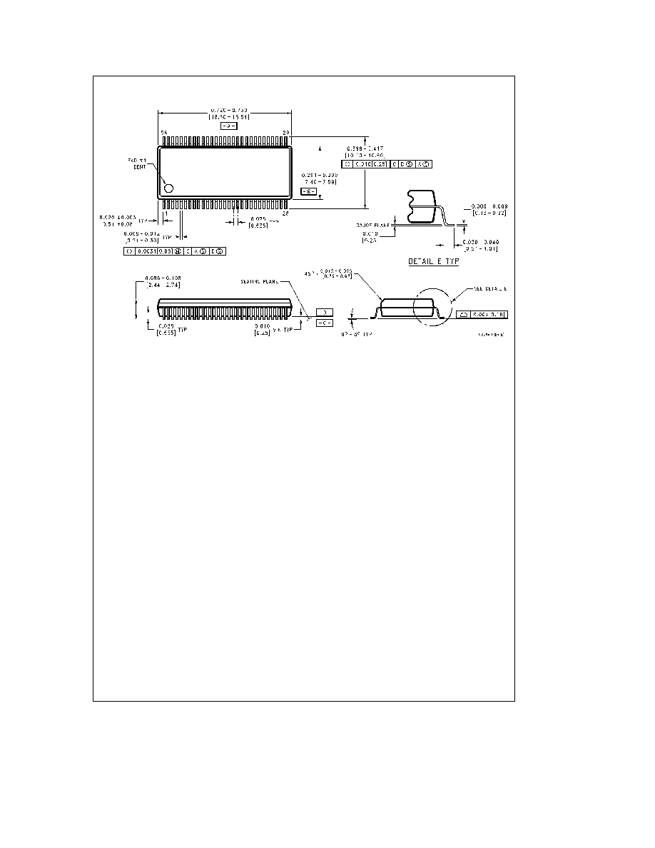
Physical Dimensions
inches (millimeters) unless otherwise noted
56-Lead Molded Shrink Small Outline Package EIAJ
Order Number 74LVT16652MEA or 74LVT16652MEAX
NS Package Number MS56A
http
www national com
5
