TL F 11639
74VHC541
Octal
BufferLine
Driver
with
TRI-STATE
Outputs
November 1995
74VHC541
Octal Buffer Line Driver with TRI-STATE
Outputs
General Description
The VHC541 is an advanced high-speed CMOS device fab-
ricated with silicon gate CMOS technology It achieves the
high-speed operation similar to equivalent Bipolar Schottky
TTL while maintaining the CMOS low power dissipation
The VHC541 is an octal buffer line driver designed to be
employed as memory and address drivers clock drivers and
bus oriented transmitter receivers
This device is similar in function to the VHC244 while provid-
ing flow-through architecture (inputs on opposite side from
outputs) This pinout arrangement makes this device espe-
cially useful as an output port for microprocessors allowing
ease of layout and greater PC board density
An input protection circuit insures that 0V to 7V can be ap-
plied to the input pins without regard to the supply voltage
This device can be used to interface 5V to 3V systems and
two supply systems such as battery backup This circuit pre-
vents device destruction due to mismatched supply and in-
put voltages
Features
Y
Low power dissipation
I
CC
e
4 mA (max) at T
A
e
25 C
Y
High noise immunity V
NIH
e
V
NIL
e
28% V
CC
(min)
Y
All inputs are equipped with a power down protection
function
Y
Balanced propagation delays t
PLH
j
t
PHL
Y
Low noise V
OLP
e
0 9V (typ)
Y
Pin and function compatible with 74HC541
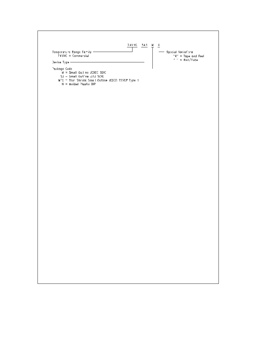
Commercial
Package Number
Package Description
74VHC541M
M20B
20-Lead Molded JEDEC SOIC
74VHC541SJ
M20D
20-Lead Molded EIAJ SOIC
74VHC541MTC
MTC20
20-Lead Molded JEDEC Type 1 TSSOP
74VHC541N
N20A
20-Lead Molded DIP
Note
Surface mount packages are also available on Tape and Reel Specify by appending the suffix letter ``X'' to the ordering code
Logic Symbol
IEEE IEC
TL F 11639 ≠ 1
Connection Diagram
Pin Assignment for DIP
TSSOP and SOIC
TL F 11639 ≠ 2
Truth Table
Inputs
Outputs
OE
1
OE
2
I
L
L
H
H
H
X
X
Z
X
H
X
Z
L
L
L
L
H
e
HIGH Voltage Level
L
e
LOW Voltage Level
X
e
Immaterial
Z
e
High Impedance
TRI-STATE
is a registered trademark of National Semiconductor Corporation
C1995 National Semiconductor Corporation
RRD-B30M125 Printed in U S A

Absolute Maximum Ratings
(Note 1)
Supply Voltage (V
CC
)
b
0 5V to
a
7 0V
DC Input Voltage (V
IN
)
b
0 5V to
a
7 0V
DC Output Voltage (V
OUT
)
b
0 5V to V
CC
a
0 5V
Input Diode Current (I
IK
)
b
20 mA
Output Diode Current (I
OK
)
g
20 mA
DC Output Current (I
OUT
)
g
25 mA
DC V
CC
GND Current (I
CC
)
g
75 mA
Storage Temperature (T
STG
)
b
65 C to
a
150 C
Lead Temperature (T
L
)
(Soldering 10 seconds)
260 C
Note 1
Absolute Maximum Ratings are values beyond
which the device may be damaged or have its useful life
impaired The databook specifications should be met with-
out exception to ensure that the system design is reliable
over its power supply temperature and output input load-
ing variables National does not recommend operation out-
side databook specifications
Recommended Operating
Conditions
Supply Voltage (V
CC
)
2 0V to
a
5 5V
Input Voltage (V
IN
)
0V to
a
5 5V
Output Voltage (V
OUT
)
0V to V
CC
Operating Temperature (T
OPR
)
b
40 C to
a
85 C
Input Rise and Fall Time (t
r
t
f
)
V
CC
e
3 3V
g
0 3V
0 E 100 ns V
V
CC
e
5 0V
g
0 5V
0 E 20 ns V
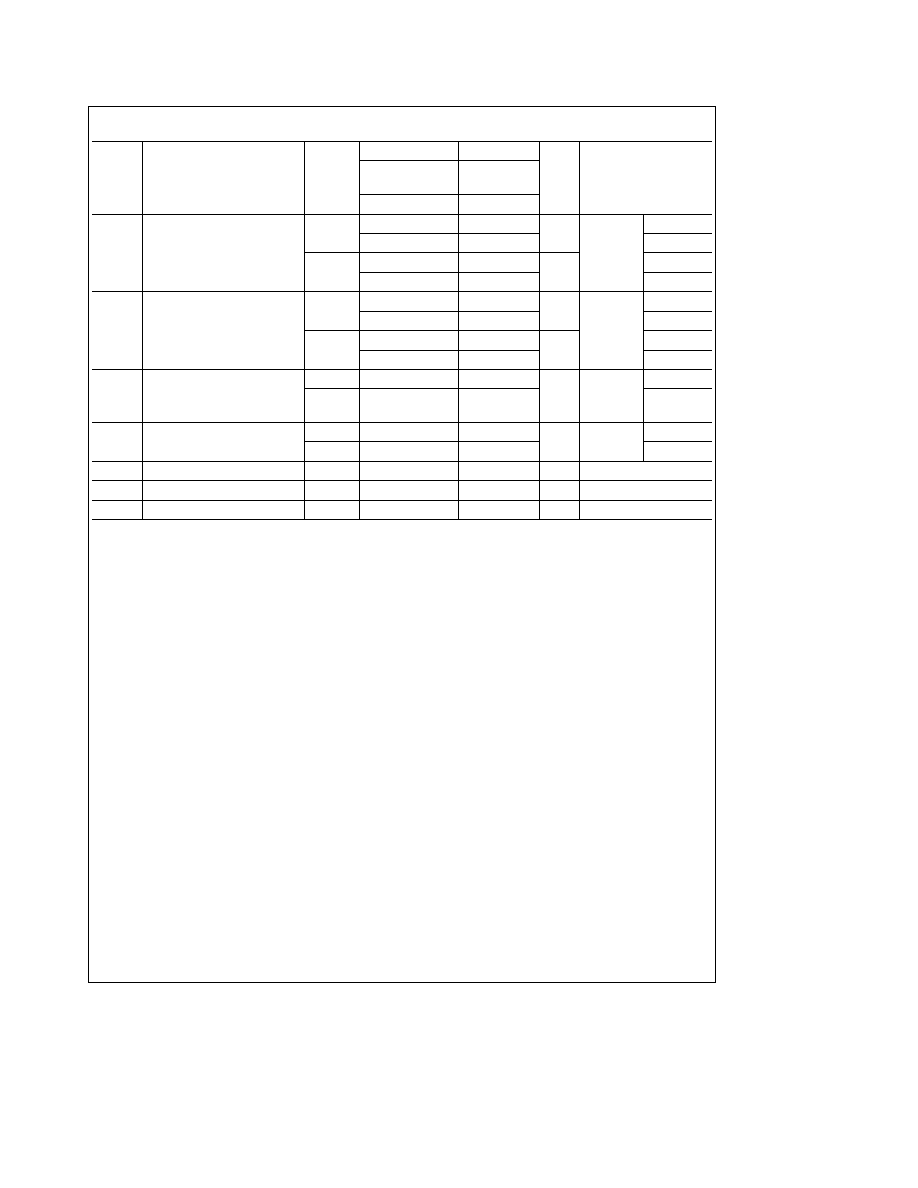
DC Characteristics for 'VHC Family Devices
Symbol
Parameter
V
CC
(V)
74VHC
Units
Conditions
T
A
e
25 C
T
A
e b
40 C
to
a
85 C
Min
Typ
Max
Min
Max
V
IH
High Level Input
2 0
1 50
1 50
V
Voltage
3 0 ≠ 5 5
0 7 V
CC
0 7 V
CC
V
IL
Low Level Input
2 0
0 50
0 50
V
Voltage
3 0 ≠ 5 5
0 3 V
CC
0 3 V
CC
V
OH
High Level Output
2 0
1 9
2 0
1 9
V
IN
e
V
IH
I
OH
e b
50 mA
Voltage
3 0
2 9
3 0
2 9
V
or V
IL
4 5
4 4
4 5
4 4
3 0
2 58
2 48
V
I
OH
e b
4 mA
4 5
3 94
3 80
I
OH
e b
8 mA
V
OL
Low Level Output
2 0
0 0
0 1
0 1
V
IN
e
V
IH
I
OL
e
50 mA
Voltage
3 0
0 0
0 1
0 1
V
or V
IL
4 5
0 0
0 1
0 1
3 0
0 36
0 44
V
I
OL
e
4 mA
4 5
0 36
0 44
I
OL
e
8 mA
I
OZ
TRI-STATE Output
5 5
g
0 25
g
2 5
m
A
V
IN
e
V
IH
or V
IL
Off-State Current
V
OUT
e
V
CC
or GND
I
IN
Input Leakage
0 ≠ 5 5
g
0 1
g
1 0
m
A
V
IN
e
5 5V or GND
Current
I
CC
Quiescent Supply
5 5
4 0
40 0
m
A
V
IN
e
V
CC
or GND
Current
2

DC Characteristics for 'VHC Family Devices
74VHC
Symbol
Parameter
V
CC
T
A
e
25 C
Units
Conditions
(V)
Typ
Limits
V
OLP
Quiet Output Maximum Dynamic
5 0
0 9
1 2
V
C
L
e
50 pF
V
OL
V
OLV
Quiet Output Minimum Dynamic
5 0
b
0 8
b
1 0
V
C
L
e
50 pF
V
OL
V
IHD
Minimum High Level Dynamic
5 0
3 5
V
C
L
e
50 pF
Input Voltage
V
ILD
Maximum High Level Dynamic
5 0
1 5
V
C
L
e
50 pF
Input Voltage
Parameter guaranteed by design
3
AC Electrical Characteristics for 'VHC Family Devices
Symbol
Parameter
V
CC
(V)
74VHC
74VHC
Units
Conditions
T
A
e
25 C
T
A
e b
40 C
to
a
85 C
Min
Typ
Max
Min
Max
t
PLH
Propagation Delay Time
3 3
g
0 3
5 0
7 0
1 0
8 5
ns
C
L
e
15 pF
t
PHL
7 5
10 5
1 0
12 0
C
L
e
50 pF
5 0
g
0 5
3 5
5 0
1 0
6 0
ns
C
L
e
15 pF
5 0
7 0
1 0
8 0
C
L
e
50 pF
t
PZL
TRI-STATE Output Enable
3 3
g
0 3
6 8
10 5
1 0
12 5
ns
R
L
e
1 kX
C
L
e
15 pF
Time
t
PZH
9 3
14 0
1 0
16 0
C
L
e
50 pF
5 0
g
0 5
4 7
7 2
1 0
8 5
ns
C
L
e
15 pF
6 2
9 2
1 0
10 5
C
L
e
50 pF
t
PLZ
TRI-STATE
3 3
g
0 3
11 2
15 4
1 0
17 5
ns
R
L
e
1 kX
C
L
e
50 pF
t
PHZ
Output
5 0
g
0 5
6 0
8 8
1 0
10 0
C
L
e
50 pF
Disable Time
t
OSLH
Output to Output Skew
3 3
g
0 3
1 5
1 5
ns
(Note 1)
C
L
e
50 pF
t
OSHL
5 0
g
0 5
1 0
1 0
C
L
e
50 pF
C
IN
Input Capacitance
4
10
10
pF
V
CC
e
Open
C
OUT
Output Capacitance
6
pF
V
CC
e
5 0V
C
PD
Power Dissipation Capacitance
18
pF
(Note 2)
Note 1
Parameter guaranteed by design t
OSLH
e
l
t
PLHmax
b
t
PLHmin
l
t
OSHL
e
l
t
PHLmax
b
t
PHLmin
l
Note 2
C
PD
is defined as the value of the internal equivalent capacitance which is calculated from the operating current consumption without load Average
operating current can be obtained by the equation I
CC
(OPR )
e
C
PD
V
CC
f
IN
a
I
CC
8 (per bit)
4