TL F 11679
74VHC943
300
Baud
Modem
(5V
Supply)
PRELIMINARY
October 1995
74VHC943
300 Baud Modem (5V Supply)
General Description
The 74VHC943 is a full duplex low speed modem It pro-
vides a 300 baud bidirectional serial interface for data com-
munication over telephone lines and other narrow band-
width channels It is Bell 103 compatible
The 74VHC943 utilizes advanced silicon-gate CMOS tech-
nology Switched capacitor techniques are used to perform
analog signal processing
MODULATOR SECTION
The modulator contains a frequency synthesizer and a sine
wave synthesizer It produces a phase coherent frequency
shift keyed (FSK) output
LINE DRIVER AND HYBRID SECTION
The line driver and hybrid are designed to facilitate connec-
tion to a 600X phone line They can perform two to four wire
conversion and drive the line at a maximum of
b
9 dBm
DEMODULATOR SECTION
The demodulator incorporates anti-aliasing filters a receive
filter limiter discriminator and carrier detect circuit The
nine-pole receive filter provides 60 dB of transmitted tone
rejection The discriminator is fully balanced for stable
operation
Features
Y
5V supply
Y
Drives 600X at
b
9 dBm
Y
All filters on chip
Y
Transmit level adjustment compatible with universal
service order code
Y
TTL and CMOS compatible logic
Y
All inputs protected against static damage
Y
Low power consumption
Y
Full duplex answer or originate operation
Y
Analog loopback for self test
Y
Power down mode
Y
Direct Pin and function replacement for the 74HC943
Applications
Y
Built-in low speed modems
Y
Remote data collection
Y
Radio telemetry
Y
Credit verification
Y
Stand-alone modems
Y
Point-of-sale terminals
Y
Tone signaling systems
Y
Remote process control
Commercial
Package Number
Package Description
74VHC943WM
M20B
20-Lead Molded JEDEC SOIC (0 300 Wide)
74VHC943N
N20A
20-Lead Molded DIP
Note
Surface mount packages are also available on Tape and Reel Specify by appending the suffix letter
``X'' to the ordering code
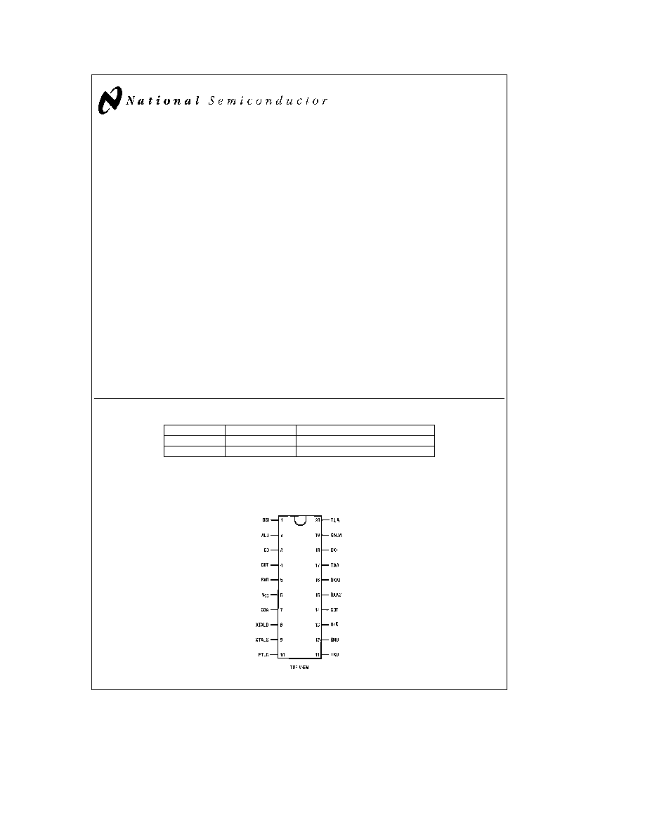
Connection Diagram
Pin Assignments for
SOIC and PDIP
TL F 11679 � 1
TRI-STATE
is a registered trademark of National Semiconductor Corporation
C1995 National Semiconductor Corporation
RRD-B30M125 Printed in U S A
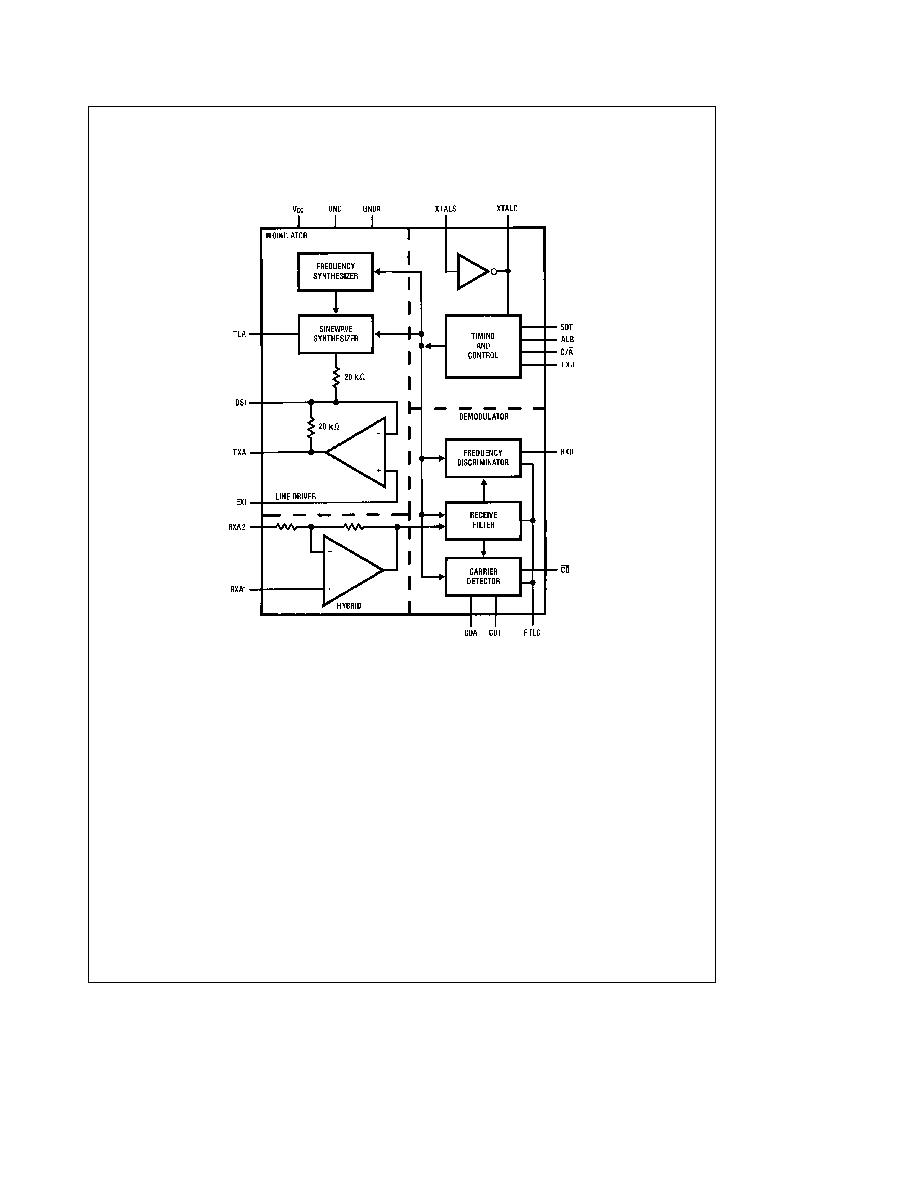
Block Diagram
TL F 11679 � 2
2

Description of Pin Functions
Pin
Name
Function
No
1
DSI
Driver Summing Input This input may be
used to transmit externally generated tones
such as dual tone multifrequency (DTMF) di-
aling signals
2
ALB
Analog Loop Back A logic high on this pin
causes the modulator output to be connect-
ed to the demodulator input so that data is
looped back through the entire chip This is
used as a chip self test If ALB and SQT are
simultaneously held high the chip powers
down
3
CD
Carrier Detect This pin goes to a logic low
when carrier is sensed by the carrier detect
circuit
4
CDT
Carrier Detect Timing A capacitor on this
pin sets the time interval that the carrier
must be present before the CD goes low
5
RXD
Received Data This is the data output pin
6
V
CC
Positive Supply Pin A
a
5V supply is recom-
mended
7
CDA
Carrier Detect Adjust This is used for ad-
justment of the carrier detect threshold Car-
rier detect hysteresis is set at 3 dB
8
XTALD
Crystal Drive XTALD and XTALS connect
to a 3 5795 MHz crystal to generate a crys-
tal locked clock for the chip If an external
circuit requires this clock XTALD should be
sensed If a suitable clock is already avail-
able in the system XTALD can be driven
9
XTALS
Crystal Sense Refer to pin 8 for details
Pin
Name
Function
No
10
FTLC
Filter Test Limiter Capacitor This is con-
nected to a high impedance output of the
receiver filter It may thus be used to evalu-
ate filter performance This pin may also be
driven to evaluate the demodulator RXA1
and RXA2 must be grounded during this
test
For normal modem operation FTLC is AC
grounded via a 0 1 mF bypass capacitor
11
TXD
Transmitted Data This is the data input
12
GND
Ground This defines the chip 0V
13
O A
Originate Answer mode select When logic
high this pin selects the originate mode of
operation
14
SQT
Squelch Transmitter This disables the mod-
ulator when held high The EXI input re-
mains active If SQT and ALB are simulta-
neously held high the chip powers down
15
RXA2
Receive Analog
2 RXA2 and RXA1 are
analog inputs When connected as recom-
mended they produce a 600X hybrid
16
RXA1
Receive Analog
1 See RXA2 for details
17
TXA
Transmit Analog This is the output of the
line driver
18
EXI
External Input This is a high impedance in-
put to the line driver This input may be used
to transmit externally generated tones
When not used for this purpose it should be
grounded to GNDA
19
GNDA
Analog Ground Analog signals within the
chip are referred to this pin
20
TLA
Transmit Level Adjust A resistor from this
pin to V
CC
sets the transmit level
3

Functional Description
INTRODUCTION
A modem is a device for transmitting and receiving serial
data over a narrow bandwidth communication channel The
74VHC943 uses frequency shift keying (FSK) of audio fre-
quency tone
The tone may be transmitted over the
switched telephone network and other voice grade chan-
nels The 74VHC943 is also capable of demodulating FSK
signals By suitable tone allocation and considerable signal
processing the 74VHC943 is capable of transmitting and
receiving data simultaneously
The tone allocation used by the 74VHC943 and other Bell
103 compatible modems is shown in Table I The terms
``originate'' and ``answer'' which define the frequency allo-
cation come from use with telephones The modem on the
end of the line which initiates the call is called the originate
modem The other modem is the answer modem
TABLE I Bell 103 Tone Allocation
Originate Modem
Answer Modem
Data
Transmit
Receive
Transmit
Receive
Space
1070 Hz
2025 Hz
2025 Hz
1070 Hz
Mark
1270 Hz
2225 Hz
2225 Hz
1270 Hz
THE LINE INTERFACE
The line interface section performs two to four wire conver-
sion and provides impedance matching between the mo-
dem and the phone line
THE LINE DRIVER
The line driver is a power amplifier for driving the line If the
modem is operating as an originate modem the second har-
monics of the transmitted tones fall close to the frequencies
of the received tones and degrade the received signal to
noise ratio (SNR) The line driver must thus produce low
second harmonic distortion
THE HYBRID
The voltage on the telephone line is the sum of the transmit-
ted and received signals The hybrid subtracts the transmit-
ted voltage from the voltage on the telephone line If the
telephone line was matched to the hybrid impedance the
output of the hybrid would be only the received signal This
rarely happens because telephone line characteristic im-
pedances vary considerably The hybrid output is thus a
mixture of transmitted and received signals
THE DEMODULATOR SECTION
The Receive Filter
The demodulator recovers the data from the received sig-
nals The signal from the hybrid is a mixture of transmitted
signal received signals and noise The first stage of the
receive filter is an anti-alias filter which attenuates high fre-
quency noise before sampling occurs The signal then goes
to the second stage of the receive filter where the transmit-
ted tones and other noise are filtered from the received sig-
nal This is a switch capacitor nine pole filter providing at
least 60 dB of transmitted tone rejection This also provides
high attenuation at 60 Hz a common noise component
The Discriminator
The first stage of the discriminator is a hard limiter The hard
limiter removes from the received signal any amplitude
modulation which may bias the demodulator toward a mark
or a space It compares the output of the receive filter to the
voltage on the 0 1 mF capacitor on the FTLC pin
The hard limiter output connects to two parallel bandpass
filters in the discriminator One filter is tuned to the mark
frequency and the other to the space frequency The out-
puts of these filters are rectified filtered and compared If
the output of the mark path exceeds the output of the space
path the RXD output goes high The opposite case sends
RXD low
The demodulator is implemented using precision switched
capacitor techniques The highly critical comparators in the
limiter and discriminator are auto-zeroed for low offset
Carrier Detector
The output of the discriminator is meaningful only if there is
sufficient carrier being received This is established in the
carrier detection circuit which measures the signal on the
line If this exceeds a certain level for a preset period (ad-
justable by the CDT pin) the CD output goes low indicating
that carrier is present Then the carrier detect threshold is
lowered by 3 dB This provides hysteresis ensuring the CD
output remains stable If carrier is lost CD goes high after
the preset delay and the threshold is increased by 3 dB
MODULATOR SECTION
The modulator consists of a frequency synthesizer and a
sine wave synthesizer The frequency synthesizer produces
one of four tones depending on the O A and TXD pins The
frequencies are synthesized to high precision using a crystal
oscillator and variable dual modulus counter
The counters used respond quickly to data changes introduc-
ing negligible bit jitter while maintaining phase coherence
The sine wave synthesizer uses switched capacitors to
``look up'' the voltages of the sine wave This sampled sig-
nal is then further processed by switched capacitor and
continuous filters to ensure the high spectral purity required
by FCC regulations
4

Absolute Maximum Ratings
(Notes 1
2)
Supply Voltage (V
CC
)
b
0 5 to
a
7 0V
DC Input Voltage (V
IN
)
b
1 5 to V
CC
a
1 5V
DC Output Voltage (V
OUT
)
b
0 5 to V
CC
a
0 5V
Clamp Diode Current (I
IK
I
OK
)
g
20 mA
DC Output Current per pin (I
OUT
)
g
25 mA
DC V
CC
or GND Current per pin (I
CC
)
g
50 mA
Storage Temperature Range (T
STG
)
b
65 C to
a
150 C
Power Dissipation (P
D
)
(Note 3)
600 mW
S O Package only
500 mW
Lead Temp (T
L
) (Soldering 10 seconds)
260 C
Operating Conditions
Min
Max
Units
Supply Voltage (V
CC
)
4 5
5 5
V
DC Input or Output Voltage
0
V
CC
V
(V
IN
V
OUT
)
Operating Temp Range (T
A
)
74VHC
b
40
a
85
C
Input Rise or Fall Times
(t
r
t
f
)
500
ns
Crystal frequency
3 579
MHz
DC Electrical Characteristics
V
CC
e
5V
g
10% unless otherwise specified
74VHC
74VHC
Symbol
Parameter
Conditions
T
A
e
25 C
T
A
e b
40 C to
a
85 C
Units
Typ
Guaranteed Limits
V
IH
Minimum High Level
3 15
3 15
V
Input Voltage
V
IL
Maximum Low Level
1 1
1 1
V
Input Voltage
V
OH
Minimum High Level
V
IN
e
V
IH
or V
IL
Output Voltage
l
I
OUT
l
e
20 mA
V
CC
b
0 05
V
CC
b
0 1
V
CC
b
0 1
V
l
I
OUT
l
e
4 0 mA V
CC
e
4 5V
3 84
3 7
V
OL
Maximum Low Level
V
IN
e
V
IH
or V
IL
Voltage
l
I
OUT
l
e
20 mA
0 1
0 1
V
l
I
OUT
l
e
4 0 mA V
CC
e
4 5V
0 33
0 4
I
IN
Maximum Input
V
IN
e
V
CC
or GND
g
0 1
g
1 0
m
A
Current
I
OZ
Output TRI-STATE
ALB
e
SQT
e
V
CC
Leakage Current
g
5
m
A
RXD and CD Outputs
I
CC
Maximum Quiescent
V
IH
e
V
CC
V
IL
e
GND
8 0
10 0
10 0
mA
Supply Current
ALB or SQT
e
GND
I
GNDA
Analog Ground Current
Transmit Level
e b
9 dBm
1 0
2 0
2 0
mA
I
CC
Power Down Supply Current
ALB
e
SQT
e
V
CC
300
m
A
V
IH
e
V
CC
V
IL
e
GND
Note 1
Absolute Maximum Ratings are those values beyond which damage to the device may occur
Note 2
Unless otherwise specified all voltages are referenced to ground
Note 3
Power Dissipation temperature derating
plastic ``N'' package
b
12 mW C from 65 C to 85 C
5