 | –≠–ª–µ–∫—Ç—Ä–æ–Ω–Ω—ã–π –∫–æ–º–ø–æ–Ω–µ–Ω—Ç: 7812 | –°–∫–∞—á–∞—Ç—å:  PDF PDF  ZIP ZIP |
LM78XX
Series Voltage Regulators
General Description
The LM78XX series of three terminal regulators is available
with several fixed output voltages making them useful in a
wide range of applications. One of these is local on card
regulation, eliminating the distribution problems associated
with single point regulation. The voltages available allow
these regulators to be used in logic systems, instrumenta-
tion, HiFi, and other solid state electronic equipment. Al-
though designed primarily as fixed voltage regulators these
devices can be used with external components to obtain ad-
justable voltages and currents.
The LM78XX series is available in an aluminum TO-3 pack-
age which will allow over 1.0A load current if adequate heat
sinking is provided. Current limiting is included to limit the
peak output current to a safe value. Safe area protection for
the output transistor is provided to limit internal power dissi-
pation. If internal power dissipation becomes too high for the
heat sinking provided, the thermal shutdown circuit takes
over preventing the IC from overheating.
Considerable effort was expanded to make the LM78XX se-
ries of regulators easy to use and minimize the number of
external components. It is not necessary to bypass the out-
put, although this does improve transient response. Input by-
passing is needed only if the regulator is located far from the
filter capacitor of the power supply.
For output voltage other than 5V, 12V and 15V the LM117
series provides an output voltage range from 1.2V to 57V.
Features
n
Output current in excess of 1A
n
Internal thermal overload protection
n
No external components required
n
Output transistor safe area protection
n
Internal short circuit current limit
n
Available in the aluminum TO-3 package
Voltage Range
LM7805C
5V
LM7812C
12V
LM7815C
15V
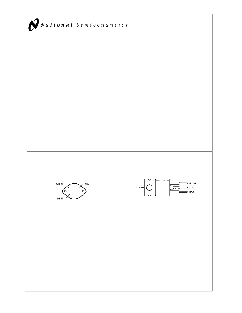
Connection Diagrams
Metal Can Package
TO-3 (K)
Aluminum
DS007746-2
Bottom View
Order Number LM7805CK,
LM7812CK or LM7815CK
See NS Package Number KC02A
Plastic Package
TO-220 (T)
DS007746-3
Top View
Order Number LM7805CT,
LM7812CT or LM7815CT
See NS Package Number T03B
May 2000
LM78XX
Series
V
oltage
Regulators
© 2000 National Semiconductor Corporation
DS007746
www.national.com
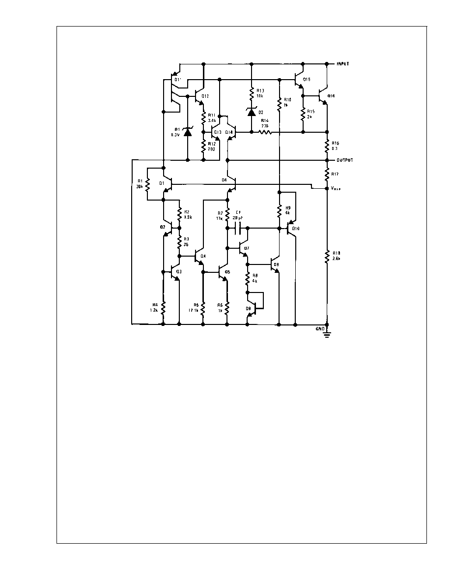
Schematic
DS007746-1
LM78XX
www.national.com
2
Absolute Maximum Ratings
(Note 3)
If Military/Aerospace specified devices are required,
please contact the National Semiconductor Sales Office/
Distributors for availability and specifications.
Input Voltage
(V
O
= 5V, 12V and 15V)
35V
Internal Power Dissipation (Note 1)
Internally Limited
Operating Temperature Range (T
A
)
0∞C to +70∞C
Maximum Junction Temperature
(K Package)
150∞C
(T Package)
150∞C
Storage Temperature Range
-65∞C to +150∞C
Lead Temperature (Soldering, 10 sec.)
TO-3 Package K
300∞C
TO-220 Package T
230∞C
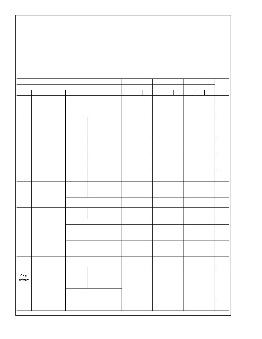
Electrical Characteristics LM78XXC
(Note 2)
0∞C
T
J
125∞C unless otherwise noted.
Output Voltage
5V
12V
15V
Input Voltage (unless otherwise noted)
10V
19V
23V
Units
Symbol
Parameter
Conditions
Min
Typ
Max
Min
Typ
Max
Min
Typ
Max
V
O
Output Voltage
Tj = 25∞C, 5 mA
I
O
1A
4.8
5
5.2
11.5
12
12.5
14.4
15
15.6
V
P
D
15W, 5 mA
I
O
1A
4.75
5.25
11.4
12.6 14.25
15.75
V
V
MIN
V
IN
V
MAX
(7.5
V
IN
20)
(14.5
V
IN
27)
(17.5
V
IN
30)
V
V
O
Line Regulation
I
O
= 500
mA
Tj = 25∞C
3
50
4
120
4
150
mV
V
IN
(7
V
IN
25)
14.5
V
IN
30)
(17.5
V
IN
30)
V
0∞C
Tj
+125∞C
50
120
150
mV
V
IN
(8
V
IN
20)
(15
V
IN
27)
(18.5
V
IN
30)
V
I
O
1A
Tj = 25∞C
50
120
150
mV
V
IN
(7.5
V
IN
20)
(14.6
V
IN
27)
(17.7
V
IN
30)
V
0∞C
Tj
+125∞C
25
60
75
mV
V
IN
(8
V
IN
12)
(16
V
IN
22)
(20
V
IN
26)
V
V
O
Load Regulation
Tj = 25∞C
5 mA
I
O
1.5A
10
50
12
120
12
150
mV
250 mA
I
O
750 mA
25
60
75
mV
5 mA
I
O
1A, 0∞C
Tj
+125∞C
50
120
150
mV
I
Q
Quiescent Current
I
O
1A
Tj = 25∞C
8
8
8
mA
0∞C
Tj
+125∞C
8.5
8.5
8.5
mA
I
Q
Quiescent Current
5 mA
I
O
1A
0.5
0.5
0.5
mA
Change
Tj = 25∞C, I
O
1A
1.0
1.0
1.0
mA
V
MIN
V
IN
V
MAX
(7.5
V
IN
20)
(14.8
V
IN
27)
(17.9
V
IN
30)
V
I
O
500 mA, 0∞C
Tj
+125∞C
1.0
1.0
1.0
mA
V
MIN
V
IN
V
MAX
(7
V
IN
25)
(14.5
V
IN
30)
(17.5
V
IN
30)
V
V
N
Output Noise
Voltage
T
A
=25∞C, 10 Hz
f
100 kHz
40
75
90
µV
Ripple Rejection
I
O
1A, Tj = 25∞C
or
62
80
55
72
54
70
dB
f = 120 Hz
I
O
500 mA
62
55
54
dB
0∞C
Tj
+125∞C
V
MIN
V
IN
V
MAX
(8
V
IN
18)
(15
V
IN
25)
(18.5
V
IN
28.5)
V
R
O
Dropout Voltage
Tj = 25∞C, I
OUT
= 1A
2.0
2.0
2.0
V
Output Resistance
f = 1 kHz
8
18
19
m
LM78XX
www.national.com
3
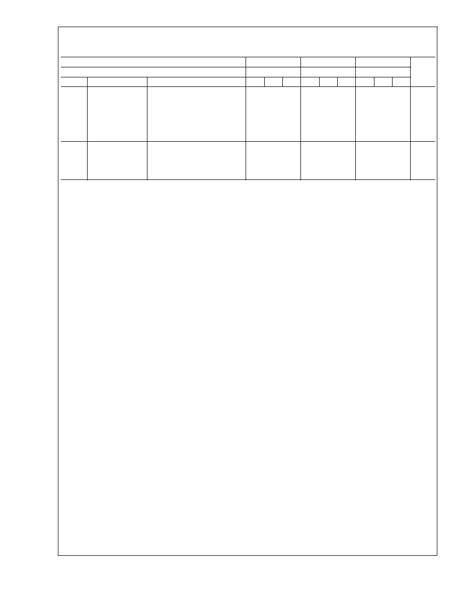
Electrical Characteristics LM78XXC
(Note 2) (Continued)
0∞C
T
J
125∞C unless otherwise noted.
Output Voltage
5V
12V
15V
Input Voltage (unless otherwise noted)
10V
19V
23V
Units
Symbol
Parameter
Conditions
Min
Typ
Max
Min
Typ
Max
Min
Typ
Max
Short-Circuit
Current
Tj = 25∞C
2.1
1.5
1.2
A
Peak Output
Current
Tj = 25∞C
2.4
2.4
2.4
A
Average TC of
V
OUT
0∞C
Tj
+125∞C, I
O
= 5 mA
0.6
1.5
1.8
mV/∞C
V
IN
Input Voltage
Required to
Maintain
Tj = 25∞C, I
O
1A
7.5
14.6
17.7
V
Line Regulation
Note 1: Thermal resistance of the TO-3 package (K, KC) is typically 4∞C/W junction to case and 35∞C/W case to ambient. Thermal resistance of the TO-220 package
(T) is typically 4∞C/W junction to case and 50∞C/W case to ambient.
Note 2: All characteristics are measured with capacitor across the input of 0.22 µF, and a capacitor across the output of 0.1µF. All characteristics except noise voltage
and ripple rejection ratio are measured using pulse techniques (t
w
10 ms, duty cycle
5%). Output voltage changes due to changes in internal temperature must
be taken into account separately.
Note 3: Absolute Maximum Ratings indicate limits beyond which damage to the device may occur. For guaranteed specifications and the test conditions, see Elec-
trical Characteristics.
LM78XX
www.national.com
4
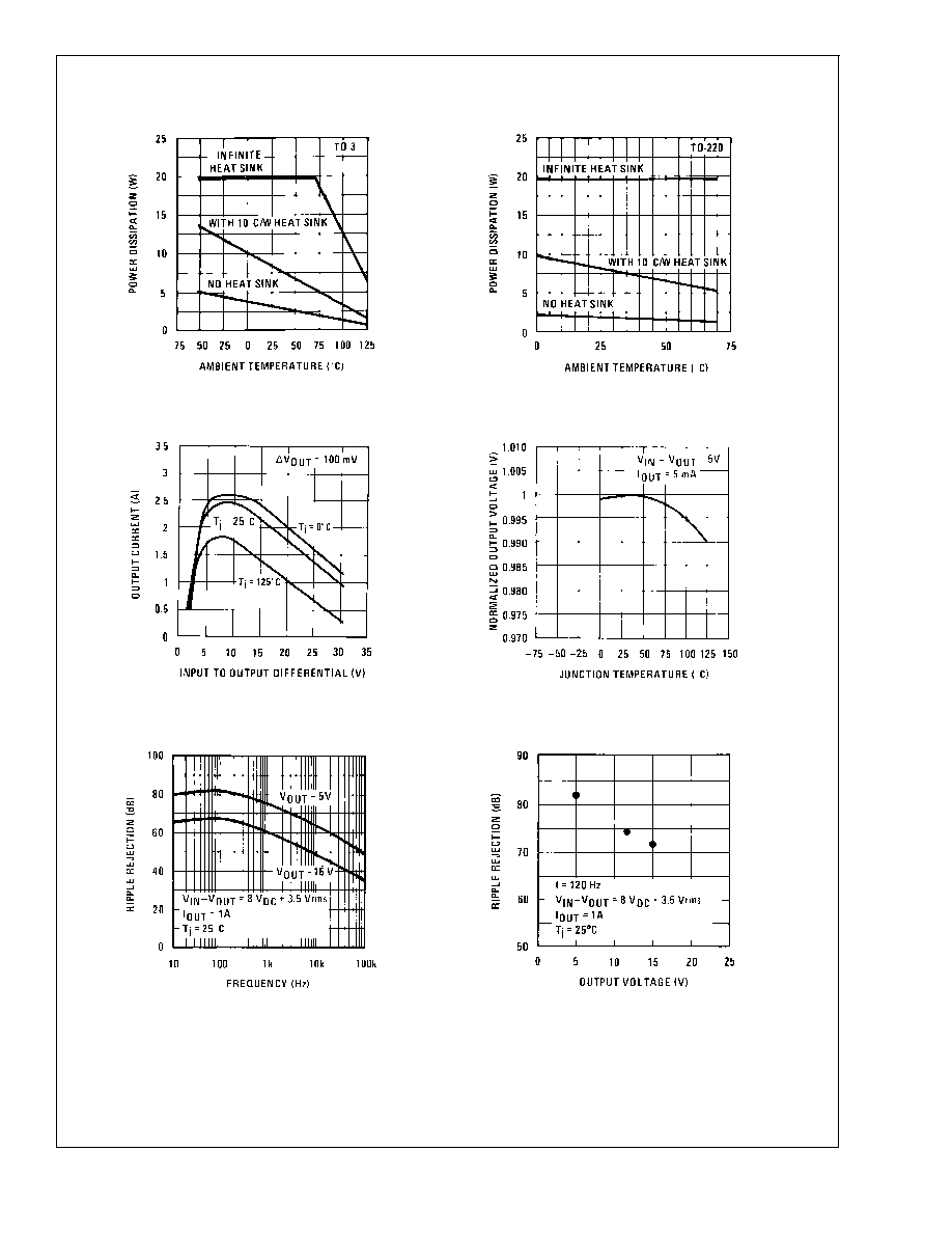
Typical Performance Characteristics
Maximum Average Power Dissipation
DS007746-5
Maximum Average Power Dissipation
DS007746-6
Peak Output Current
DS007746-7
Output Voltage (Normalized to 1V at T
J
= 25∞C)
DS007746-8
Ripple Rejection
DS007746-9
Ripple Rejection
DS007746-10
LM78XX
www.national.com
5