 | –≠–ª–µ–∫—Ç—Ä–æ–Ω–Ω—ã–π –∫–æ–º–ø–æ–Ω–µ–Ω—Ç: 9338 | –°–∫–∞—á–∞—Ç—å:  PDF PDF  ZIP ZIP |
TL F 9794
9338DM9338
8-Bit
Multiple
Port
Register
June 1989
9338 DM9338 8-Bit Multiple Port Register
General Description
The DM9338 is an 8-bit multiple port register designed for
high speed random access memory applications where the
ability to simultaneously read and write is desirable A com-
mon use would be as a register bank in a three address
computer Data can be written into any one of the eight bits
and read from any two of the eight bits simultaneously
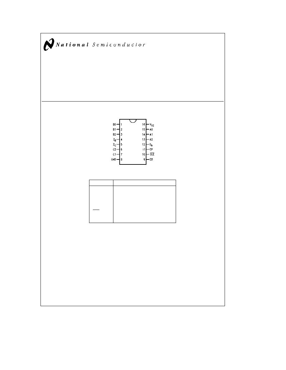
Connection Diagrams
Dual-In-Line Package
TL F 9794 ≠ 1
Order Number 9338DMQB 9338FMQB or DM9338N
See NS Package Number J16A N16E or W16A
Pin Names
Description
A0 ≠ A2
Write Address Inputs
D
A
Data Input
B0 ≠ B2
B Read Address Inputs
C0 ≠ C2
C Read Address Inputs
CP
Clock Pulse Input (Active Rising Edge)
SLE
Slave Enable Input (Active LOW)
Z
B
B Output
Z
C
C Output
FAST
and TRI-STATE
are registered trademarks of National Semiconductor Corporation
C1995 National Semiconductor Corporation
RRD-B30M115 Printed in U S A
Absolute Maximum Ratings
(Note)
If Military Aerospace specified devices are required
please contact the National Semiconductor Sales
Office Distributors for availability and specifications
Supply Voltage
7V
Input Voltage
5 5V
Operating Free Air Temperature Range
Military
b
55 C to
a
125 C
Commercial
0 C to
a
70 C
Storage Temperature Range
b
65 C to
a
150 C
Note
The ``Absolute Maximum Ratings'' are those values
beyond which the safety of the device cannot be guaran-
teed The device should not be operated at these limits The
parametric values defined in the ``Electrical Characteristics''
table are not guaranteed at the absolute maximum ratings
The ``Recommended Operating Conditions'' table will define
the conditions for actual device operation
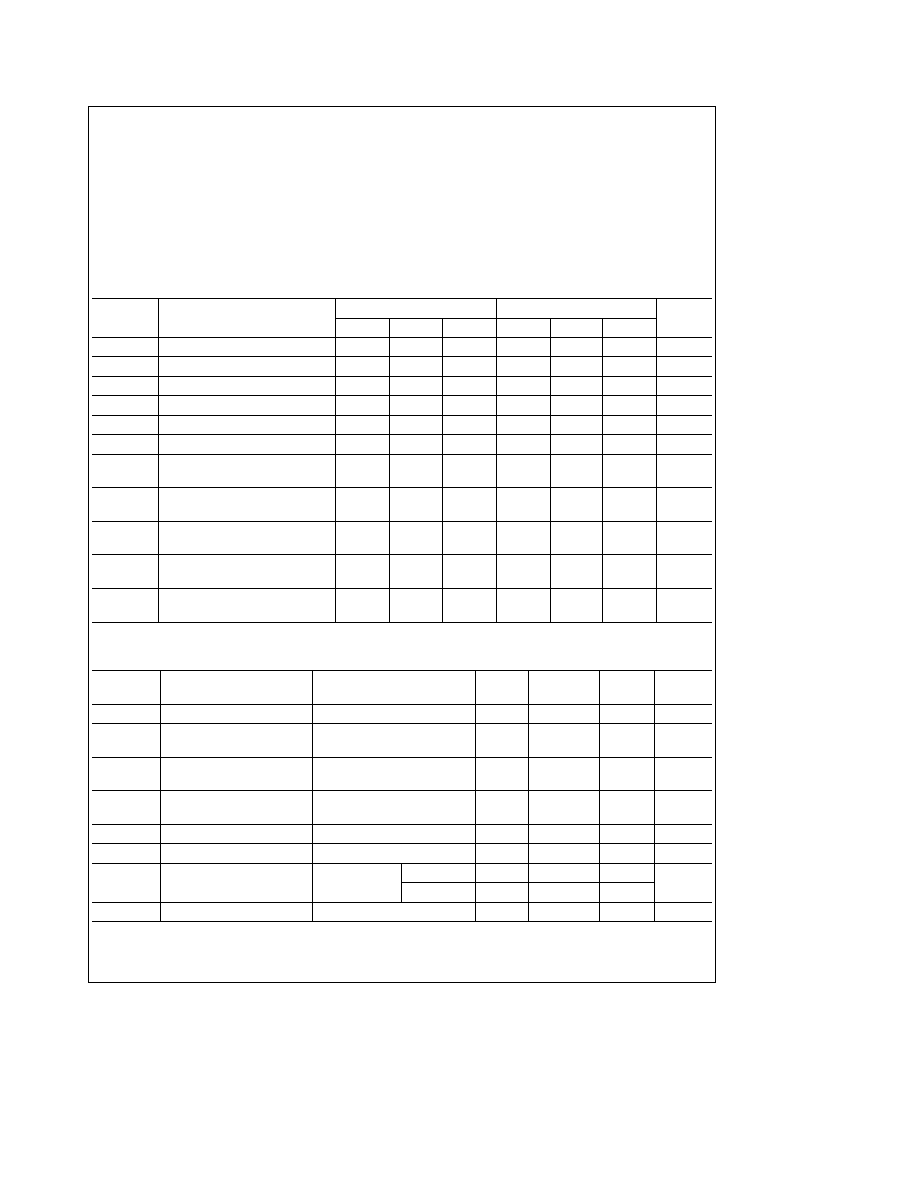
Recommended Operating Conditions
Symbol
Parameter
Military
Commercial
Units
Min
Nom
Max
Min
Nom
Max
V
CC
Supply Voltage
4 5
5
5 5
4 75
5
5 25
V
V
IH
High Level Input Voltage
2
2
V
V
IL
Low Level Input Voltage
0 8
0 8
V
I
OH
High Level Output Current
b
0 8
b
0 8
mA
I
OL
Low Level Output Current
16
16
mA
T
A
Free Air Operating Temperature
b
55
125
0
70
C
t
s
(H)
Setup Time HIGH or LOW
20
20
ns
t
s
(L)
D
A
to CP
12
12
t
h
(H)
Hold Time HIGH or LOW
0
0
ns
t
h
(L)
D
A
to CP
b
8 0
b
8 0
t
s
(H)
Setup Time HIGH or LOW
10
10
ns
t
s
(L)
A
n
to CP
10
10
t
h
(H)
Hold Time HIGH or LOW
0
0
ns
t
h
(L)
A
n
to CP
0
0
t
w
(H)
CP Pulse Width HIGH or LOW
23
23
ns
t
w
(L)
13
13
Electrical Characteristics
Over recommended operating free air temperature range (unless otherwise noted)
Symbol
Parameter
Conditions
Min
Typ
Max
Units
(Note 1)
V
I
Input Clamp Voltage
V
CC
e
Min I
I
e b
12 mA
b
1 5
V
V
OH
High Level Output Voltage
V
CC
e
Min I
OH
e
Max
2 4
3 4
V
V
IL
e
Max
V
OL
Low Level Output Voltage
V
CC
e
Min I
OL
e
Max
0 2
0 4
V
V
IH
e
Min
I
I
Input Current
Max
V
CC
e
Max V
I
e
5 5V
1
mA
Input Voltage
I
IH
High Level Input Current
V
CC
e
Max V
I
e
2 4V
27
m
A
I
IL
Low Level Input Current
V
CC
e
Max V
I
e
0 4V
b
1 1
mA
I
OS
Short Circuit
V
CC
e
Max
MIL
b
10
b
70
mA
Output Current
(Note 2)
COM
b
10
b
70
I
CC
Supply Current
V
CC
e
Max
135
mA
Note 1
All typicals are at V
CC
e
5V T
A
e
25 C
Note 2
Not more than one output should be shorted at a time
2
Switching Characteristics
V
CC
e a
5 0V T
A
e a
25 C (See Section 1 for waveforms and load configurations)
C
L
e
15 pF
Symbol
Parameter
9338 (MIL)
DM9338 (COM)
Units
Min
Max
Min
Max
t
PLH
Propagation Delay
40
13
40
ns
t
PHL
B
n
or C
n
to Z
n
35
18
35
t
PLH
Propagation Delay
45
25
45
ns
t
PHL
D
A
to Z
n
50
25
50
t
PLH
Propagation Delay
35
18
35
ns
t
PHL
CP to Z
n
30
13
30
Functional Description
The 9338 8-bit multiple port register can be considered a 1-
bit slice of eight high speed working registers Data can be
written into any one and read from any two of the eight
locations simultaneously Master slave operation eliminates
all race problems associated with simultaneous read write
activity from the same location When the clock input (CP) is
LOW data applied to the data input line (D
A
) enters the
selected master This selection is accomplished by coding
the three write input select lines (A0 ≠ A2) appropriately
Data is stored synchronously with the rising edge of the
clock pulse
The information for each of the two slaved (output) latches
is selected by two sets of read address inputs (B0 ≠ B2 and
C0 ≠ C2) The information enters the slave while the clock is
HIGH and is stored while the clock is LOW If Slave Enable
is LOW (SLE) the slave latches are continuously enabled
The signals are available on the output pins (Z
B
and Z
C
)
The input bit selection and the two output bit selections can
be accomplished independently or simultaneously The data
flows into the device is demultiplexed according to the state
of the write address lines and is clocked into the selected
latch The eight latches function as masters and store the
input data The two output latches are slaves and hold the
data during the read operation The state of each slave is
determined by the state of the master selected by its associ-
ated set of read address inputs
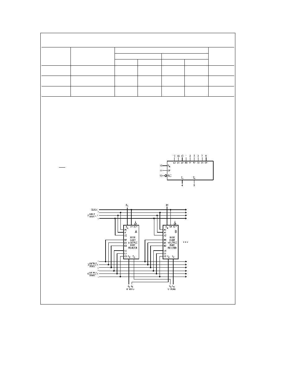
The method of parallel expansion is shown in
Figure a One
9338 is needed for each bit of the required word length The
read and write input lines should be connected in common
on all of the devices This register configuration provides
two words of n-bits each at one time where n devices are
connected in parallel
Logic Symbol
TL F 9794 ≠ 2
V
CC
e
Pin 16
GND
e
Pin 8
TL F 9794 ≠ 4
FIGURE a Parallel Expansion
3
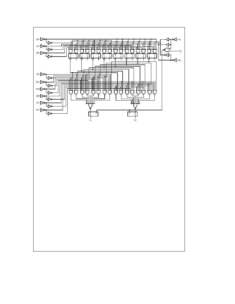
Logic Diagram
TL F 9794 ≠ 3
4
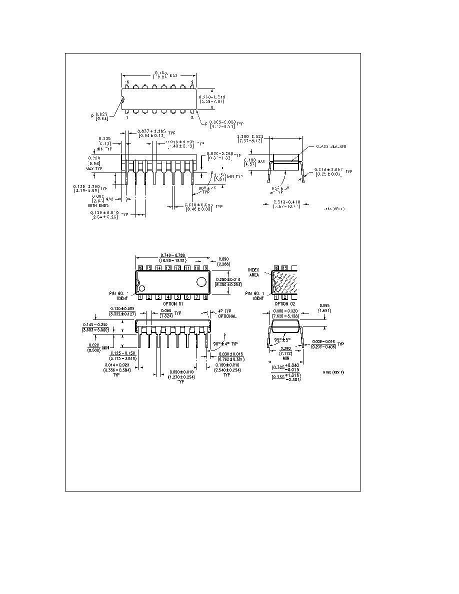
Physical Dimensions
inches (millimeters)
16-Lead Ceramic Dual-In-Line Package (J)
Order Number 9338DMQB
NS Package Number J16A
16-Lead Molded Dual-In-Line Package (N)
Order Number DM9338N
NS Package Number N16E
5

9338DM9338
8-Bit
Multiple
Port
Register
Physical Dimensions
inches (millimeters) (Continued)
16-Lead Ceramic Flat Package (W)
Order Number 9338FMQB
NS Package Number W16A
LIFE SUPPORT POLICY
NATIONAL'S PRODUCTS ARE NOT AUTHORIZED FOR USE AS CRITICAL COMPONENTS IN LIFE SUPPORT
DEVICES OR SYSTEMS WITHOUT THE EXPRESS WRITTEN APPROVAL OF THE PRESIDENT OF NATIONAL
SEMICONDUCTOR CORPORATION As used herein
1 Life support devices or systems are devices or
2 A critical component is any component of a life
systems which (a) are intended for surgical implant
support device or system whose failure to perform can
into the body or (b) support or sustain life and whose
be reasonably expected to cause the failure of the life
failure to perform when properly used in accordance
support device or system or to affect its safety or
with instructions for use provided in the labeling can
effectiveness
be reasonably expected to result in a significant injury
to the user
National Semiconductor
National Semiconductor
National Semiconductor
National Semiconductor
Corporation
Europe
Hong Kong Ltd
Japan Ltd
1111 West Bardin Road
Fax (a49) 0-180-530 85 86
13th Floor Straight Block
Tel 81-043-299-2309
Arlington TX 76017
Email cnjwge tevm2 nsc com
Ocean Centre 5 Canton Rd
Fax 81-043-299-2408
Tel 1(800) 272-9959
Deutsch Tel (a49) 0-180-530 85 85
Tsimshatsui Kowloon
Fax 1(800) 737-7018
English
Tel (a49) 0-180-532 78 32
Hong Kong
Fran ais Tel (a49) 0-180-532 93 58
Tel (852) 2737-1600
Italiano
Tel (a49) 0-180-534 16 80
Fax (852) 2736-9960
National does not assume any responsibility for use of any circuitry described no circuit patent licenses are implied and National reserves the right at any time without notice to change said circuitry and specifications