TL F 10203
96L02DM96L02
Dual
Retriggerable
Resettable
Monostable
Multivibrator
March 1992
96L02 DM96L02
Dual Retriggerable Resettable
Monostable Multivibrator
General Description
The 96L02 is a dual TTL monostable multivibrator with trig-
ger mode selection reset capability rapid recovery inter-
nally compensated reference levels and high speed capabil-
ity Output pulse duration and accuracy depend on external
timing components and are therefore under user control for
each application It is well suited for a broad variety of appli-
cations including pulse delay generators square wave gen-
erators long delay timers pulse absence detectors fre-
quency detectors clock pulse generators and fixed-frequen-
cy dividers Each input is provided with a clamp diode to
limit undershoot and minimize ringing induced by fast fall
times acting on system wiring impedances
Features
Y
Retriggerable 0% to 100% duty cycle
Y
DC level triggering insensitive to transition times
Y
Leading or trailing-edge triggering
Y
Complementary outputs with active pull-ups
Y
Pulse width compensation for DV
CC
and DT
A
Y
50 ns to % output pulse width range
Y
Optional retrigger lock-out capability
Y
Resettable for interrupt operations
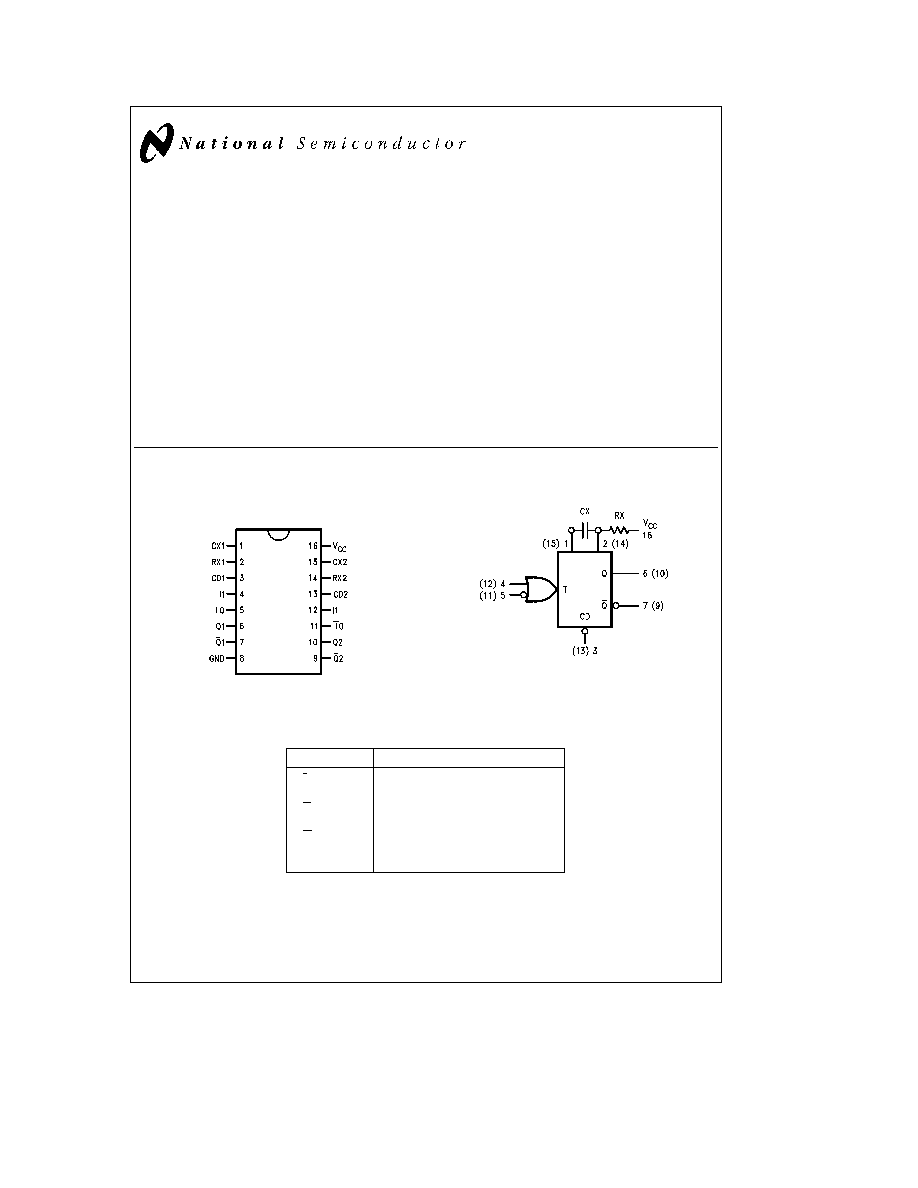
Connection Diagram
Dual-In-Line Package
TL F 10203 � 1
Order Number 96L02DMQB
96L02FMQB or DM96L02N
See NS Package Number J16A N16E or W16A
Logic Symbol
TL F 10203 � 2
V
CC
e
Pin 16
GND
e
Pin 8
Pin Names
Description
I0
Trigger Input (Active Falling Edge)
I1
Trigger Input (Active Rising Edge)
C
D
Direct Clear Input (Active LOW)
Q
Positive Pulse Output
Q
Complementary Pulse Output
CX
External Capacitor Connection
RX
External Resistor Connection
C1995 National Semiconductor Corporation
RRD-B30M105 Printed in U S A
Absolute Maximum Ratings
(Note)
If Military Aerospace specified devices are required
please contact the National Semiconductor Sales
Office Distributors for availability and specifications
Supply Voltage
7V
Input Voltage
5 5V
Operating Free Air Temperature Range
Military
b
55 C to
a
125 C
Commercial
0 C to
a
70 C
Storage Temperature Range
b
65 C to
a
150
Note
The ``Absolute Maximum Ratings'' are those values
beyond which the safety of the device cannot be guaran-
teed The device should not be operated at these limits The
parametric values defined in the ``Electrical Characteristics''
table are not guaranteed at the absolute maximum ratings
The ``Recommended Operating Conditions'' table will define
the conditions for actual device operation
Recommended Operating Conditions
Symbol
Parameter
Conditions
96L02 (Mil)
DM96L02 (Com)
Units
Min
Nom
Max
Min
Nom
Max
V
CC
Supply Voltage
4 5
5
5 5
4 75
5
5 25
V
V
IH
High Level Input Voltage
2
2
V
V
IL
Low Level Input Voltage
0 7
0 7
V
I
OH
High Level Output Current
0 36
0 36
mA
I
OL
Low Level Output Current
4 8
4 8
mA
T
A
Free Air Operating
b
55
125
0
70
C
Temperature
t
w
(L)
Minimum Input Pulse
V
CC
e
5 0V
50
ns
t
w
(H)
Width I1 I0
t
w
(min)
Minimum Output Pulse
V
CC
e
5 0V
Width at Q Q
R
X
e
20 kX
10
300
110
ns
C
X
e
0
C
L
e
15 pF
t
w
Output Pulse Width Q Q
V
CC
e
5 0V
R
X
e
39 kX
11 5
14 2
12 4
15 2
m
s
C
X
e
1000 pF
R
X
Timing Resistor Range
100
220
kX
Electrical Characteristics
over recommended operating free air temperature (unless otherwise noted)
Symbol
Parameter
Conditions
Min
Typ
Max
Units
(Note 1)
V
I
Input Clamp Voltage
V
CC
e
Min I
I
e b
10 mA
b
1 5
V
V
OH
High Level Output Voltage
V
CC
e
Min I
OH
e
Max
2 4
V
V
IL
e
Max V
IH
e
Min
V
OL
Low Level Output Voltage
V
CC
e
Min I
OL
e
Max
0 3
V
V
IL
e
Min V
IL
e
Max
I
I
Input Current
Max
V
CC
e
Max V
I
e
5 5V
1
mA
Input Voltage
I
IH
High Level Input Current
V
CC
e
Max V
I
e
2 4V
20
m
A
I
IL
Low Level Input Current
V
CC
e
Max V
I
e
0 3V
b
0 4
mA
I
OS
Short Circuit Output Current
V
CC
e
Max (Note 2) V
O
e
1 0V
b
2 0
b
13 0
mA
I
CC
Supply Current
V
CC
e
Max (Note 3)
16
mA
Note 1
All typicals are at V
CC
e
5V T
A
e
25 C
Note 2
Not more than one output should be shorted at a time and the duration should not exceed one second
Note 3
I
CC
is measured with all outputs open and all inputs grounded
2
Switching Characteristics
V
CC
e a
5 0V T
A
e a
25 C
Symbol
Parameter
Conditions
96L02 (Mil)
DM96L02 (Com)
Units
Min
Max
Min
Max
t
PLH
Propagation Delay I0 to Q
V
CC
e
5 0V R
X
e
20 kX
75
80
ns
I1 to Q
C
X
e
0 C
L
e
15 pF
t
PHL
Propagation Delay I0 to Q
V
CC
e
5 0V R
X
e
20 kX
62
65
ns
I1 to Q
C
X
e
0 C
L
e
15 pF
t
PLH
Propagation Delay CD to Q
V
CC
e
5 0V R
X
e
39 kX
100
ns
t
PHL
CD to Q
C
X
e
1000 pF
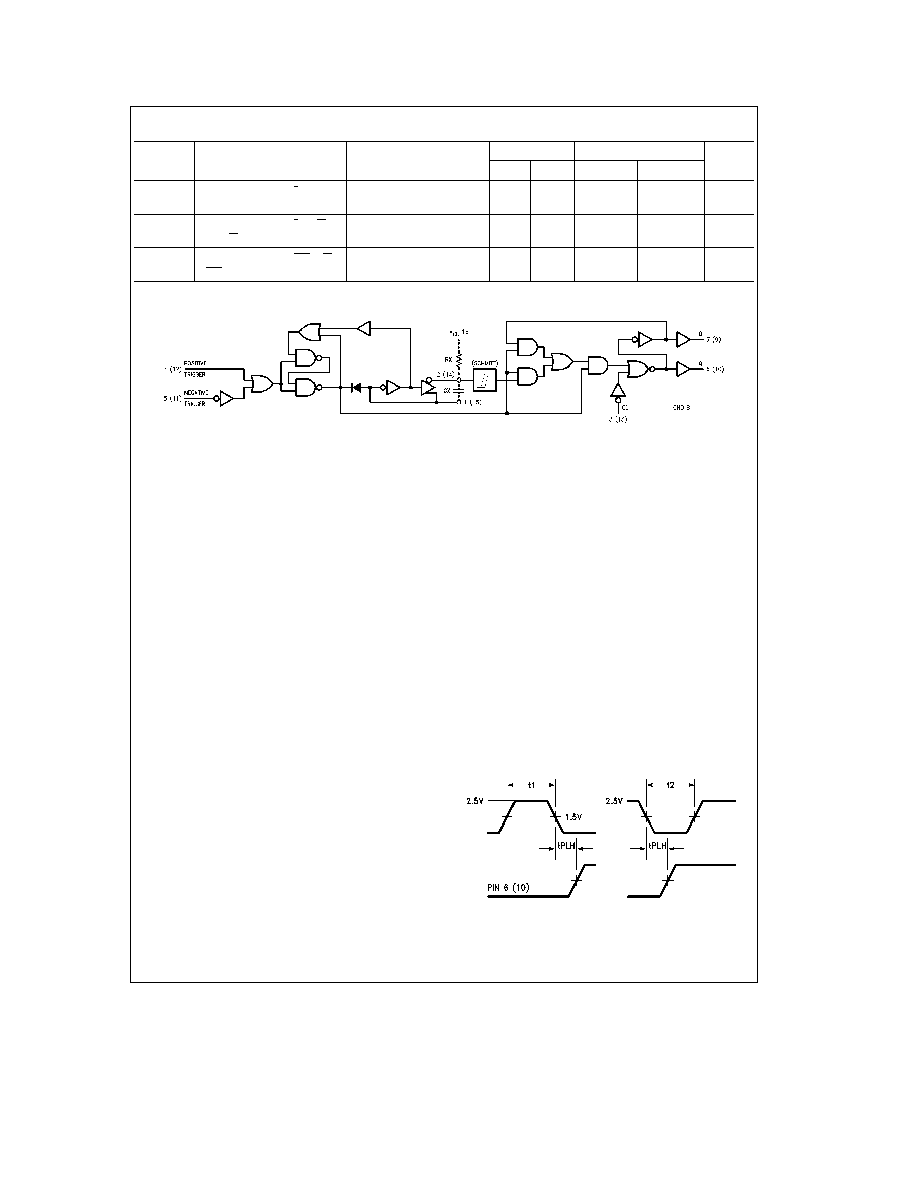
Functional Block Diagram
TL F 10203 � 3
Operation Notes
1 TRIGGERING
can be accomplished by a positive-going
transition on pin 4 (12) or a negative-going transition on
pin 5 (11) Triggering begins as a signal crosses the input
V
IL
V
IH
threshold region this activates an internal latch
whose unbalanced cross-coupling causes it to assume a
preferred state As the latch output goes LOW it disables
the gates leading to the Q output and through an invert-
er turns on the capacitor discharge transistor The invert-
ed signal is also fed back to the latch input to change its
state and effectively end the triggering action thus the
latch and its associated feed-back perform the function of
a differentiator
The emitters of the latch transistors return to ground
through an enabling transistor which must be turned off
between successive triggers in order for the latch to pro-
ceed through the proper sequence when triggering is de-
sired Pin 5 (11) must be HIGH in order to trigger at pin 4
(12) conversely pin 4 (12) must be LOW in order to trig-
ger at pin 5 (11)
2 RETRIGGERING
In a normal cycle triggering initiates a
rapid discharge of the external timing capacitor followed
by a ramp voltage run-up at pin 2 (14) The delay will time
out when the ramp voltage reaches the upper trigger
point of a Schmitt circuit causing the outputs to revert to
the quiescent state If another trigger occurs before the
ramp voltage reaches the Schmitt threshold the capaci-
tor will be discharged and the ramp will start again without
having disturbed the output The delay period can there-
fore be extended for an arbitrary length of time by insur-
ing that the interval between triggers is less than the de-
lay time as determined by the external capacitor and re-
sistor
3 NON-RETRIGGERABLE OPERATION
Retriggering can
be inhibited logically by connecting pin 6 (10) back to pin
4 (12) or by connecting pin 7 (9) back to pin 5 (11) Either
hook-up has the effect of keeping the latch-enabling tran-
sistor turned on during the delay period which prevents
the input latch from cycling as discussed above in the
section on triggering
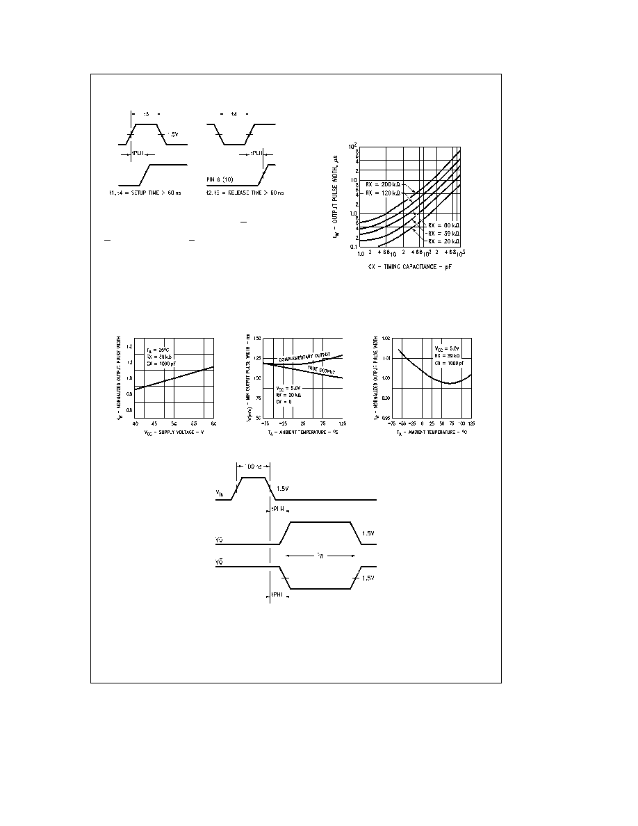
4 OUTPUT PULSE WIDTH
An external resistor R
X
and an
external capacitor C
X
are required as shown in the func-
tional block diagram To minimize stray capacitance and
noise pickup R
X
and C
X
should be located as close as
possible to the circuit In applications which require re-
mote trimming of the pulse width as with a variable resis-
tor R
X
should consist of a fixed resistor in series with the
variable resistor the fixed resistor should be located as
close as possible to the circuit The output pulse width t
w
is defined as follows where R
X
is in kX C
X
is in pF and
t
w
is in ns
t
w
e
0 33 R
X
C
X
(1
a
3 R
X
) for C
X
t
10
3
pF
16 kX
s
R
X
s
220 kX for 0 C to
a
75 C
20 kX
s
R
X
s
100 kX for
b
55 C to
a
125 C
C
X
may vary from 0 to any value For pulse widths with C
X
less than 10
3
pF see
Figure a
5 SETUP AND RELEASE TIMES
The setup times listed
below are necessary to allow the latch-enabling transistor
to turn off and the node voltages within the input latch to
stabilize thus insuring proper cycling of the latch when
the next trigger occurs The indicated release times
(equivalent to trigger duration) allow time for the input
latch to cycle and its signal to propagate
Input to Pin 5 (11)
TL F 10203 � 4
Pin 4 (12)
e
L
Pin 3 (13)
e
H
3
Operation Notes
(Continued)
TL F 10203 � 5
Input to Pin 4 (12)
Pins 5 (11) and 3 (13)
e
H
6 RESET OPERATION
A LOW signal on C
D
pin 3 (13)
will terminate an output pulse causing Q to go LOW and
Q to go HIGH As long as C
D
is held LOW a delay period
cannot be initiated nor will attempted triggering cause
spikes at the outputs A reset pulse duration in the LOW
state of 25 ns is sufficient to insure resetting If the reset
input goes LOW at the same time that a trigger transition
occurs the reset will dominate and the outputs will not
respond to the trigger If the reset input goes HIGH coinci-
dent with a trigger transition the circuit will respond to the
trigger
96L02 Pulse Width vs R
X
and C
X
TL F 10203 � 6
FIGURE a
Typical Characteristics
t
w
vs V
CC
t
w(min)
vs T
A
t
w
vs T
A
TL F 10203 � 7
INPUT PULSE
f j 25 kHz
Amp j 3 0V
Width j 100 ns
t
r
e
t
f
s
10 ns
TL F 10203 � 8
FIGURE b
4

Physical Dimensions
inches (millimeters)
16-Lead Ceramic Dual-In-Line Package (J)
Order Number 96L02DMQB
NS Package Number J16A
16-Lead Molded Dual-In-Line Package (N)
Order Number DM96L02N
NS Package Number N16E
5

96L02DM96L02
Dual
Retriggerable
Resettable
Monostable
Multivibrator
Physical Dimensions
inches (millimeters) (Continued)
16-Lead Ceramic Flat Package (W)
Order Number 96L02FMQB
NS Package Number W16A
LIFE SUPPORT POLICY
NATIONAL'S PRODUCTS ARE NOT AUTHORIZED FOR USE AS CRITICAL COMPONENTS IN LIFE SUPPORT
DEVICES OR SYSTEMS WITHOUT THE EXPRESS WRITTEN APPROVAL OF THE PRESIDENT OF NATIONAL
SEMICONDUCTOR CORPORATION As used herein
1 Life support devices or systems are devices or
2 A critical component is any component of a life
systems which (a) are intended for surgical implant
support device or system whose failure to perform can
into the body or (b) support or sustain life and whose
be reasonably expected to cause the failure of the life
failure to perform when properly used in accordance
support device or system or to affect its safety or
with instructions for use provided in the labeling can
effectiveness
be reasonably expected to result in a significant injury
to the user
National Semiconductor
National Semiconductor
National Semiconductor
National Semiconductor
Corporation
Europe
Hong Kong Ltd
Japan Ltd
1111 West Bardin Road
Fax (a49) 0-180-530 85 86
13th Floor Straight Block
Tel 81-043-299-2309
Arlington TX 76017
Email cnjwge tevm2 nsc com
Ocean Centre 5 Canton Rd
Fax 81-043-299-2408
Tel 1(800) 272-9959
Deutsch Tel (a49) 0-180-530 85 85
Tsimshatsui Kowloon
Fax 1(800) 737-7018
English
Tel (a49) 0-180-532 78 32
Hong Kong
Fran ais Tel (a49) 0-180-532 93 58
Tel (852) 2737-1600
Italiano
Tel (a49) 0-180-534 16 80
Fax (852) 2736-9960
National does not assume any responsibility for use of any circuitry described no circuit patent licenses are implied and National reserves the right at any time without notice to change said circuitry and specifications