 | –≠–ª–µ–∫—Ç—Ä–æ–Ω–Ω—ã–π –∫–æ–º–ø–æ–Ω–µ–Ω—Ç: A09A | –°–∫–∞—á–∞—Ç—å:  PDF PDF  ZIP ZIP |
LMC2001
High Precision, 6MHz Rail-To-Rail Output Operational
Amplifier
General Description
The LMC2001 is a new precision amplifier that offers un-
precedented accuracy and stability at an affordable price
and is offered in miniature (SOT23-5) package. This device
utilizes patented techniques to measure and continually cor-
rect the input offset error voltage. The result is an amplifier
which is ultra stable over time, and temperature. It has excel-
lent CMRR and PSRR ratings, and does not exhibit the fa-
miliar 1/f voltage and current noise increase that plagues tra-
ditional amplifiers. The combination of the LMC2001
characteristics makes it a good choice for transducer ampli-
fiers, high gain configurations, ADC buffer amplifiers, DAC
I-V conversion, and any other 5V application requiring preci-
sion and/or stability.
Other useful benefits of the LMC2001 are rail-to-rail output,
low supply current of 750µA, and wide gain-bandwidth
product of 6MHz. The LMC2001 comes in 5 pin SOT23 and
8 pin SOIC. These extremely versatile features found in the
LMC2001 provide high performance and ease of use.
Features
(Vs = 5V, R
L
= 10K to V
+
/2, Typ. Unless Noted)
n
Low Guaranteed V
os
40µV
n
e
n
With No 1/f
85nV/
n
High CMRR
120dB
n
High PSRR
120dB
n
High A
VOL
137dB
n
Wide Gain-Bandwidth Product
6MHz
n
High Slew Rate
5V/µs
n
Low Supply Current
750µA
n
Rail-To-Rail Output
30mV from either rail
n
No External Capacitors Required
Applications
n
Precision Instrumentation Amplifiers
n
Thermocouple Amplifiers
n
Strain Gauge Bridge Amplifier
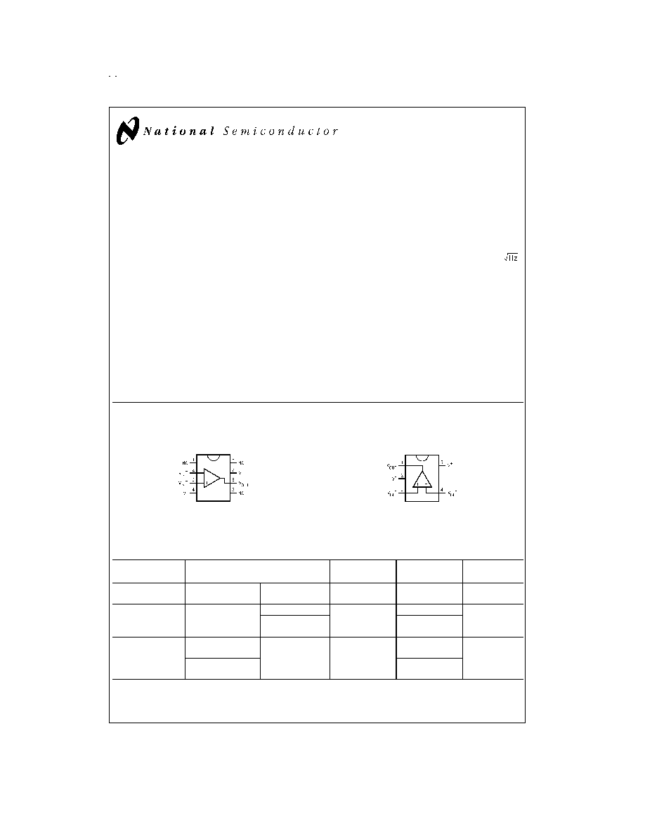
Connection Diagrams
Ordering Information
Package
Temperature Range
Package
Marking
Transport
Media
NSC
Drawing
Commercial
0∞C to +70∞C
Industrial
-40∞C to +85∞C
8-pin Small Outline
LMC2001AIM
LMC2001AIM
Rails
M08A
LMC2001AIMX
2.5k Units Tape
and Reel
5-pin SOT23-5
LMC2001ACM5
A09A
1k Units Tape
and Reel
MA05B
LMC2001ACM5X
3k Units Tape
and Reel
8-Pin SO
DS100058-1
Top View
5-Pin SOT23
DS100058-2
Top View
August 1999
LMC2001
High
Precision,
6MHz
Rail-T
o-Rail
Output
Operational
Amplifier
© 1999 National Semiconductor Corporation
DS100058
www.national.com
Absolute Maximum Ratings
(Note 1)
If Military/Aerospace specified devices are required,
please contact the National Semiconductor Sales Office/
Distributors for availability and specifications.
ESD Tolerance (Note 2)
Human Body Model
2500V
Machine Model
150V
Differential Input Voltage
±
Supply Voltage
Supply Voltage (V
+
- V
-
)
5.6V
Current At Input Pin
30mA
Current At Output Pin
30mA
Current At Power Supply Pin
(Note 3)
50mA
Lead Temperature (soldering, 10
sec)
260∞C
Storage Temperature Range
-65∞C to 150∞C
Junction Temperature (T
J
)
(Note 4)
150∞C
Operating Ratings
(Note 1)
Supply voltage
4.75V to 5.25V
Temperature Range
LMC2001AI
-40∞C
T
J
85∞C
LMC2001AC
0∞C
T
J
70∞C
Thermal resistance (
JA
)
M Package, 8-pin Surface Mount
180∞C /W
M5 Package, SOT23-5
274∞C /W
DC Electrical Characteristics
Unless otherwise specified, all limits guaranteed for T
J
= 25∞C, V
+
= 5V, V
-
= 0V, V
CM
= 2.5V, V
O
= 2.5V and R
L
>
1M
.
Boldface limits apply at the temperature extremes.
Symbol
Parameter
Conditions
Typ
(Note 5)
Limit(Note 6)
Units
V
OS
Input Offset Voltage
(Note 11)
0.5
40
60
µV
max
Offset Calibration Time
5
30
ms
TCV
OS
Input Offset Voltage
(Note 12)
0.015
µV/∞C
Long-Term Offset Drift
(Note 8)
0.006
µV/month
Lifetime V
OS
drift
(Note 8)
2.5
5
µV Max
I
IN
Input Current
(Note 9)
-3
pA
I
OS
Input Offset Current
6
pA
R
IND
Input Differential Resistance
9
M
CMRR
Common Mode Rejection
Ratio
0V
V
CM
3.5V
120
100
dB
min
0.1V
V
CM
3.5V
110
90
dB
min
PSRR
Power Supply
Rejection Ratio
4.75V
V
+
5.25V
120
95
90
dB
min
A
VOL
Large Signal Voltage Gain
(Note 7)
R
L
= 10k
137
105
100
dB
min
R
L
= 2k
128
95
90
V
O
Output Swing
R
L
= 10k
to 2.5V
V
IN
(diff) =
±
0.5V
4.975
4.955
4.955
V
min
0.030
0.060
0.060
V
max
R
L
= 2k
to 2.5V
V
IN
(diff) =
±
0.5V
4.936
V
0.075
V
I
O
Output Current
Sourcing, V
O
= 0V
V
IN
(diff) =
±
0.5V
5.9
4.1
1.5
mA
min
Sinking, V
O
= 5V
V
IN
(diff) =
±
0.5V
14.5
4.5
1.5
mA
min
I
S
Supply Current
0.75
1.0
1.2
mA
max
www.national.com
2
AC Electrical Characteristics
T
J
= 25∞C, V
+
= 5V, V
-
= 0V, V
CM
= 2.5V, V
O
= 2.5V, and R
L
>
1M
.
Symbol
Parameter
Conditions
Typ
(Note 5)
Units
SR
Slew Rate
A
V
= +1, V
in
=3.5Vpp
5
V/µs
GBW
Gain-Bandwidth Product
6
MHz
m
Phase Margin
75
Deg
G
m
Gain Margin
12
dB
e
n
Input-Referred Voltage Noise
f = 0.1Hz
85
nV/
e
n
p-p
Input-Referred Voltage Noise
R
S
= 100
, DC to 10Hz
1.6
µVpp
i
n
Input-Referred Current Noise
f = 0.1Hz
180
fA/
THD
Total Harmonic Distortion
f = 1kHz, Av = -2
R
L
= 10k
,V
O
= 4.5Vpp
0.02
%
trec
Input Overload Recovery Time
50
ms
T
S
Output Settling time
(Note 10) A
V
= +1, 1V step
1%
250
ns
0.1%
400
0.01%
3200
(Note 10)A
V
= -1, 1V step
1%
80
0.1%
860
0.01%
1400
Note 1: Absolute Maximum Ratings indicate limits beyond which damage to the device may occur. Operating Ratings indicate conditions for which the device is in-
tended to be functional, but specific performance is not guaranteed. For guaranteed specifications and test conditions, see the Electrical Characteristics.
Note 2: Human body model, 1.5k
in series with 100pF. Machine model, 200
in series with 100pF.
Note 3: Output currents in excess of
±
30mA over long term may adversely affect reliability.
Note 4: The maximum power dissipation is a function of T
J(max)
,
JA
, and T
A
. The maximum allowable power dissipation at any ambient temperature is P
D
= (T
J(max)
- T
A
)/
JA
. All numbers apply for packages soldered directly onto a PC board.
Note 5: Typical values represent the most likely parametric norm.
Note 6: All limits are guaranteed by testing or statistical analysis, unless otherwise noted.
Note 7: V
+
= 5V, V
CM
= 2.5V, and R
L
connected to 2.5V. For Sourcing tests, 2.5V
V
O
4.8V. For Sinking tests, 0.2V
V
O
2.5V.
Note 8: Guaranteed Vos Drift is based on 280 devices operated for 1000 hrs at 150∞C (equivalent to 30 years 55∫C).
Note 9: Guaranteed by design only.
Note 10: Settling times shown correspond to the worse case (positive or negative step) and does not include slew time. See the Application Note section for test
schematic.
Note 11: The limits are set by the accuracy of high speed automatic test equipment. For the typical V
OS
distribution, see the curve on page 4.
Note 12: Precision bench measurement of more than 300 units. More than 65% of units had less than 15nV /∞C V
OS
drift.
www.national.com
3
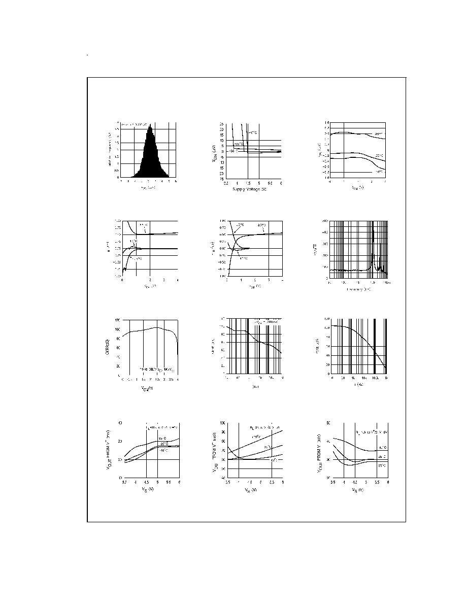
Typical Performance Characteristics
T
A
=25C, V
S
= 5V unless otherwise specified.
V
OS
Distribution
DS100058-63
V
OS
vs V
S
DS100058-91
V
OS
vs V
CM
DS100058-97
+I
IN
vs V
CM
DS100058-68
-I
IN
vs V
CM
DS100058-A4
e
N
vs Frequency
DS100058-A0
CMR vs V
CM
DS100058-92
CMR vs Frequency
DS100058-65
PSR vs Frequency
DS100058-66
V
OUT
+
vs V
S
DS100058-89
V
OUT
+
vs V
S
DS100058-88
V
OUT
-
vs V
S
DS100058-99
www.national.com
4
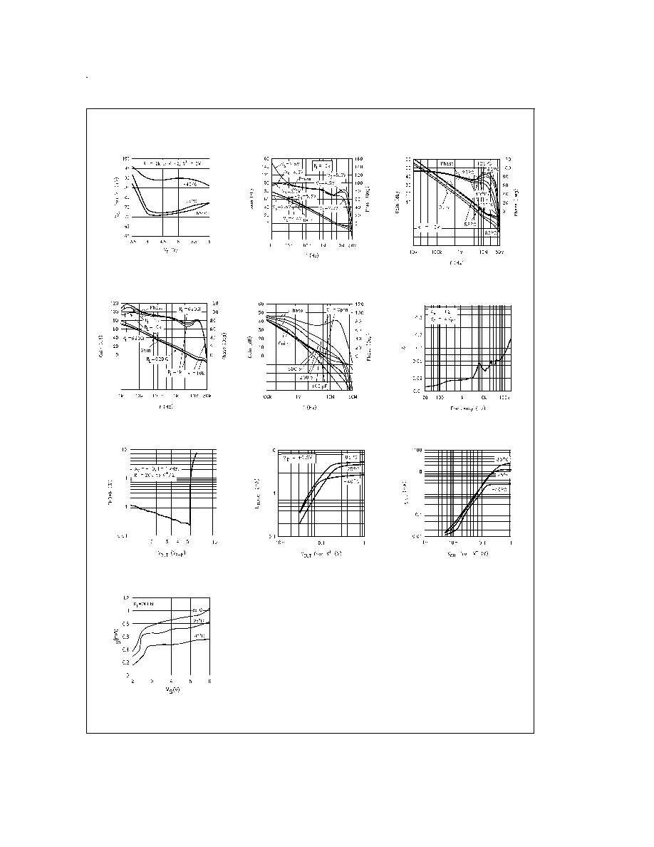
Typical Performance Characteristics
(Continued)
V
OUT
-
vs V
S
DS100058-98
Gain-Phase vs V
S
DS100058-49
Gain-Phase vs Temp
DS100058-48
Gain-Phase vs R
L
DS100058-50
Gain-Phase vs C
LOAD
DS100058-47
THD+N vs Frequency
DS100058-A5
THD+N vs V
OUT
DS100058-76
Isource vs V
OUT
DS100058-A7
Isink vs V
OUT
DS100058-A8
Isupply vs V
S
DS100058-96
www.national.com
5

Application Notes
The Benefits of LMC2001
No 1/f Noise
Using patented methods, the LMC2001 eliminates the 1/f
noise present in other amplifiers. This noise which increases
as frequency decreases is a major source of measurement
error in all DC coupled measurements. Low frequency noise
appears as a constantly changing signal in series with any
measurement being made. As a result, even when the mea-
surement is made rapidly, this constantly changing noise sig-
nal will corrupt the result. The value of this noise signal can
be surprisingly large. For example: If a conventional ampli-
fier has a high frequency noise level of 10nV/
and a
noise corner of 10 Hz, the RMS noise at 0.001 Hz is 1µV/
This is equivalent to a 6µV peak-to-peak error. In a circuit
with a gain of 1000, this produces a 6mV peak-to-peak out-
put error. This number of 0.001 Hz might appear unreason-
ably low but when a data acquisition system is operating for
17 minutes it has been on long enough to include this error.
In this same time, the LMC2001 will only have a 0.51mV out-
put error. This is more than 13.3 times less error.
Keep in mind that this 1/f error gets even larger at lower fre-
quencies.
At the extreme, many people try to reduce this error by inte-
grating or taking several samples of the same signal. This is
also doomed to failure because the 1/f nature of this noise
means that taking longer samples just moves the measure-
ment into lower frequencies where the noise level is even
higher.
The LMC2001 eliminates this source of error. The noise level
is constant with frequency so that reducing the bandwidth re-
duces the errors caused by noise.
Another source of error that is rarely mentioned is the error
voltages caused by the inadvertent thermocouples created
when the common "Kovar type" package lead materials are
soldered to a copper printed circuit board. These steel based
leadframe materials can produce over 35uV/∞C when sol-
dered onto a copper trace. This can result in thermocouple
noise that is equal to the LMC2001 noise when there is a
temperature difference of only 0.0014∞C between the lead
and the board!
For this reason, the leadframe of the LMC2001 is made of
copper. This results in equal and opposite junctions which
cancel this effect. The extremely small size of the SOT-23
package results in the leads being very close together. This
further reduces the probability of temperature differences
and hence decreases thermal noise.
Overload Recovery
The LMC2001 recovers from input overload much faster
than most chopper stabilized opamps. Recovery, from driv-
ing the amplifier to 2X the full scale output, only requires
about 50ms. Most chopper stabilized amplifiers will take
from 250ms to several seconds to recover from this same
overload. This is because large capacitors are used to store
the unadjusted offset voltage.
The wide bandwidth of the LMC2001 enhances performance
when it is used as an amplifier to drive loads that inject tran-
sients back into the output. A to Ds and multiplexers are ex-
amples of this type of load. To simulate this type of load, a
pulse generator producing a 1V peak square wave was con-
nected to the output through a 10pF capacitor. (
Figure 1)
The typical time for the output to recover to 1% of the applied
pulse is 80ns. To recover to 0.1% requires 860ns. This rapid
recovery is due to the wide bandwidth of the output stage
and large total GBW.
No External Capacitors Required
The LMC2001 does not need external capacitors. This elimi-
nates the problems caused by capacitor leakage and dielec-
tric absorption, which can cause delays of several seconds
from turn-on until the amplifier is settled.
More Benefits
The LMC2001 offers the benefits mentioned above and
more. It is rail-to-rail output and consumes only 750µA of
supply current while providing excellent DC and AC electrical
performance. In DC performance, the LMC2001 achieves
120dB of CMRR, 120dB of PSRR and 137dB of open loop
gain. In AC performance, the LMC2001 provides 6MHz of
gain-bandwidth product and 5V/µs of slew rate.
How the LMC2001 Works
The LMC2001 uses new, patented techniques to achieve the
high DC accuracy traditionally associated with chopper sta-
bilized amplifiers without the major drawbacks produced by
chopping. The LMC2001 continuously monitors the input off-
set and corrects this error. The conventional chopping pro-
cess produces many mixing products, both sums and differ-
ences, between the chopping frequency and the incoming
signal frequency. This mixing causes large amounts of dis-
tortion, particularly when the signal frequency approaches
the chopping frequency. Even without an incoming signal,
the chopper harmonics mix with each other to produce even
more trash. If this sounds unlikely or difficult to understand,
look at the plot (
Figure 2), of the output of a typical (MAX432)
chopper stabilized opamp. This is the output when there is
no incoming signal, just the amplifier in a gain of -10 with the
input grounded. The chopper is operating at about 150Hz,
the rest is mixing products. Add an input signal and the mess
gets much worse. Compare this plot with
Figure 3 of the
LMC2001. This data was taken under the exact same condi-
tions. The auto zero action is visible at about 11kHz but note
the absence of mixing products at other frequencies. As a re-
sult, the LMC2001 has very low distortion of 0.02% and very
low mixing products.
Input Currents
The LMC2001 input current is different than standard bipolar
or CMOS input currents in that it appears as a current flow-
ing in one input and out the other. Under most operating con-
ditions, these currents are in the picoamp level and will have
little or no effect in most circuits. These currents increase to
the nA level when the common-mode voltage is near the mi-
nus supply. (see the typical curves) At high temperatures
such as 85∞C, the input currents become larger, 0.5nA typi-
cal, and are both positive except when the Vcm is near V
-
. If
operation is expected at low common-mode voltages and
high temperature, do not add resistance in series with the in-
puts to balance the impedances. Doing this can cause an in-
crease in offset voltage.
DS100058-B0
FIGURE 1.
www.national.com
6

Application Notes
(Continued)
This Strain-Gauge (
Figure 4) amplifier provides high gain
(1006 or 60 dB) with very low offset and drift. Using the resis-
tors tolerance as shown, the worst case CMRR will be
greater than 90 dB. The common-mode gain is directly re-
lated to the resistor mismatch and is independent of the dif-
ferential gain that is set by R3. The worst case common-
mode gain is -54 dB. This gain becomes even lower,
improving CMRR, if the resistor ratio matching is improved.
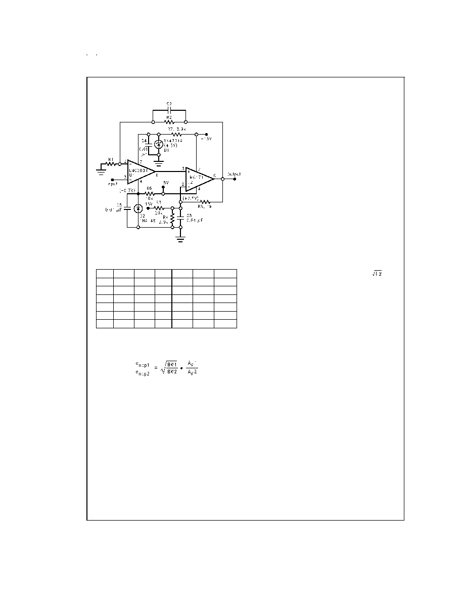
Extending Supply Voltages and Output Swing by Using
a Composite Amplifier Configuration:
In cases where substantially higher output swing is required
with higher supply voltages, arrangements like the ones
shown in
Figure 5, and Figure 6 could be used (pin numbers
shown are for SO-8 package). These configurations utilize
the excellent DC performance of the LMC2001 while at the
same time allow the superior voltage and frequency capabili-
ties of the LM6171 to set the dynamic performance of the
overall amplifier. For example, it is possible to achieve
±
12V
output swing with 300MHz of overall GBW (Av=100) while
keeping the worst case output shift due to Vos less than
4mV. The LMC2001 output voltage is kept at about mid-point
of it's overall supply voltage and it's input common mode
voltage range allows the V
-
terminal to be grounded in one
case (
Figure 5, inverting operation) and tied to a small non-
critical negative bias in another (
Figure 6, non-inverting op-
eration). Higher closed loop gains are also possible with a
corresponding reduction in realizable bandwidth. Table 1
shows some other closed loop gain possibilities along with
the measured performance in each case
Application Circuits
DS100058-A1
FIGURE 2.
DS100058-A0
FIGURE 3.
DS100058-21
FIGURE 4. Single Supply Strain- Gauge Amplifier
DS100058-30
FIGURE 5. Inverting Composite Amplifier
www.national.com
7
Application Notes
(Continued)
TABLE 1. Composite Amplifier Measured Performance
Av
R1
R2
C2
BW
SR
e
npp
(ohm)
(ohm)
(pF)
(MHz)
(V/us)
(mVpp)
50
200
10K
8
3.3
178
37
100
100
10K
10
2.5
174
70
100
1K
100K
0.67
3.1
170
70
500
200
100K
1.75
1.4
96
250
1000
100
100K
2.2
0.98
64
400
In terms of the measured output peak-to-peak noise, the fol-
lowing relationship holds between output noise voltage, e
npp
,
for different closed loop gain, A
v
, settings, where -3dB Band-
width is BW:
(1)
It should be kept in mind that in order to minimize the output
noise voltage for a given closed loop gain setting, one could
minimize the overall bandwidth. As can be seen from Equa-
tion 1 above, the improvement in output noise has a square
law relationship to the reduction in BW.
In the case of the inverting configuration, it is also possible to
increase the input impedance of the overall amplifier, by rais-
ing the value of R1, without having to increase the feedback
resistor, R2, to impractical values, by utilizing a "T" network
as feedback. See the LMC6442 data sheet (Application
Notes section) for more details on this.
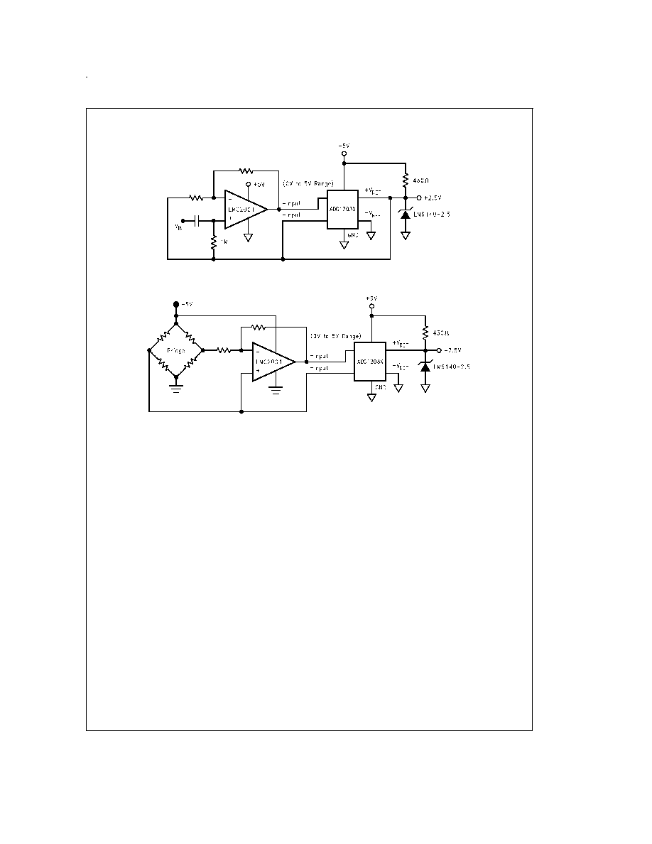
LMC2001 as ADC Input Amplifier
The LMC2001 is a great choice for an amplifier stage imme-
diately before the input of an A/D converter (AC or DC
coupled) see
Figure 7 and Figure 8 because of the following
important characteristics:
a) Very low offset voltage and offset voltage drift over time
and temperature allow a high closed loop gain setting with-
out introducing any short term or long term errors. For ex-
ample, when set to a closed loop gain of 100 as the analog
input amplifier of a 12 bit A/D converter, the overall conver-
sion error over full operation temperature and 30 years life of
the part (operating at 50∞C) would be less than 5LSB.
b) Fast large signal settling time to 0.01% of final value (1.4
us) allows 12 bit accuracy at 100KHz or more sampling rate.
c) No flicker (1/f) noise means unsurpassed data accuracy
over any measurement period of time, no matter how long.
Consider the following opamp performance, based on a typi-
cal commercially available device, for comparison:
Opamp flatband noise
8nV/
1/f
0.94
corner frequency
100Hz
f(max)
100Hz
Av
100
Measurement time
100 sec
The example above, will result in about 3mVpp (2.5LSB) of
output noise contribution due to the opamp alone, compared
to about 420 uVpp (less than 1LSB) when that opamp is re-
placed with the LMC2001 which has no 1/f contribution. If the
measurement time is increased from 100 sec. to 1 hr., the
improvement realized by using the LMC2001 would be a fac-
tor of about 44 times (18.5mVpp compared to 420uV when
LMC2001 is used) mainly because the LMC2001 accuracy is
not compromised by increasing the observation time.
d) Copper lead frame construction minimizes any thermo-
couple effects which would degrade low level/high gain data
conversion application accuracy (see discussion under "The
Benefits of the LMC2001" section above).
e) Rail-to-Rail output swing maximized the ADC dynamic
range in 5V single supply converter applications. Below are
some typical block diagrams showing the LMC2001 used as
an ADC amplifier (
Figure 7 and Figure 8).
DS100058-31
FIGURE 6. Non-Inverting Composite Amplifier
www.national.com
8
Application Notes
(Continued)
DS100058-52
FIGURE 7.
DS100058-53
FIGURE 8.
www.national.com
9
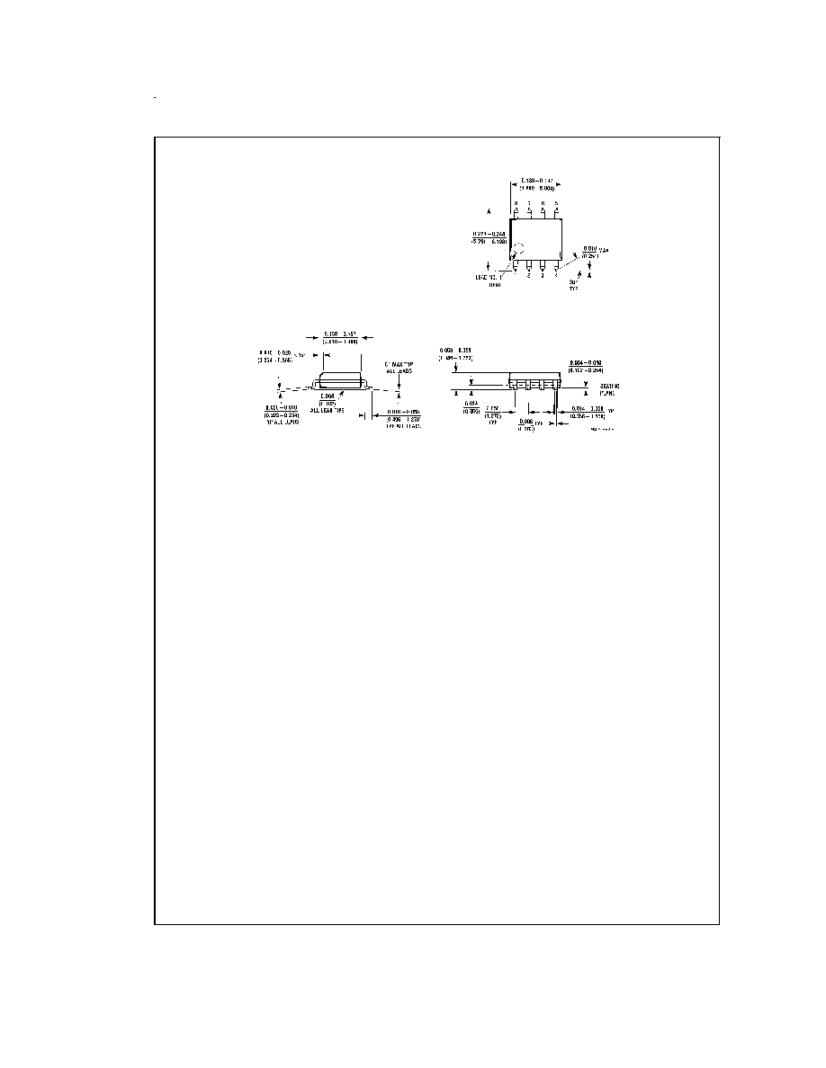
Physical Dimensions
inches (millimeters) unless otherwise noted
M08A
www.national.com
10
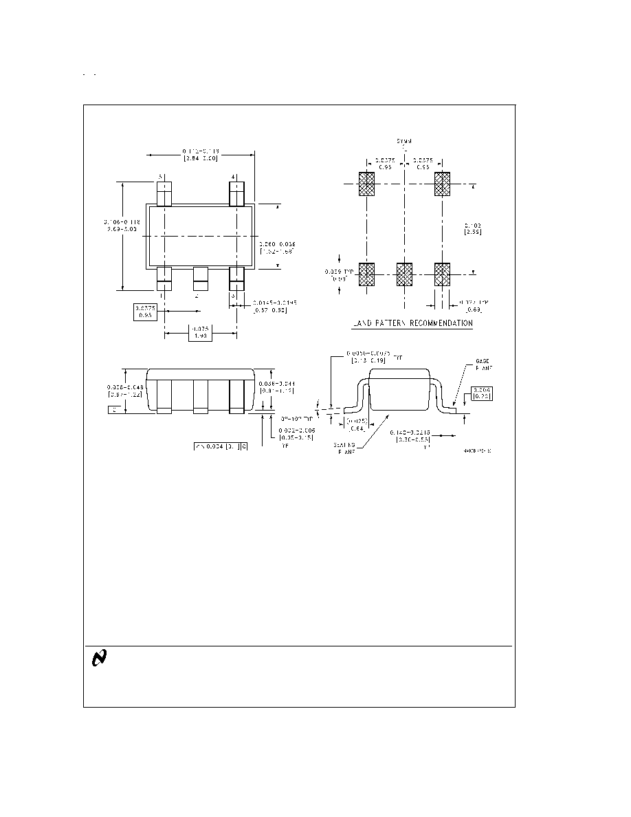
Physical Dimensions
inches (millimeters) unless otherwise noted (Continued)
LIFE SUPPORT POLICY
NATIONAL'S PRODUCTS ARE NOT AUTHORIZED FOR USE AS CRITICAL COMPONENTS IN LIFE SUPPORT
DEVICES OR SYSTEMS WITHOUT THE EXPRESS WRITTEN APPROVAL OF THE PRESIDENT AND GENERAL
COUNSEL OF NATIONAL SEMICONDUCTOR CORPORATION. As used herein:
1. Life support devices or systems are devices or
systems which, (a) are intended for surgical implant
into the body, or (b) support or sustain life, and
whose failure to perform when properly used in
accordance with instructions for use provided in the
labeling, can be reasonably expected to result in a
significant injury to the user.
2. A critical component is any component of a life
support device or system whose failure to perform
can be reasonably expected to cause the failure of
the life support device or system, or to affect its
safety or effectiveness.
National Semiconductor
Corporation
Americas
Tel: 1-800-272-9959
Fax: 1-800-737-7018
Email: support@nsc.com
National Semiconductor
Europe
Fax: +49 (0) 1 80-530 85 86
Email: europe.support@nsc.com
Deutsch Tel: +49 (0) 1 80-530 85 85
English
Tel: +49 (0) 1 80-532 78 32
FranÁais Tel: +49 (0) 1 80-532 93 58
Italiano
Tel: +49 (0) 1 80-534 16 80
National Semiconductor
Asia Pacific Customer
Response Group
Tel: 65-2544466
Fax: 65-2504466
Email: sea.support@nsc.com
National Semiconductor
Japan Ltd.
Tel: 81-3-5639-7560
Fax: 81-3-5639-7507
www.national.com
MA05B
LMC2001
High
Precision,
6MHz
Rail-T
o-Rail
Output
Operational
Amplifier
National does not assume any responsibility for use of any circuitry described, no circuit patent licenses are implied and National reserves the right at any time without notice to change said circuitry and specifications.