ADC101S051
Single Channel, 500 ksps, 10-Bit A/D Converter
General Description
The ADC101S051 is a low-power, single channel CMOS
10-bit analog-to-digital converter with a high-speed serial
interface. Unlike the conventional practice of specifying per-
formance at a single sample rate only, the ADC101S051 is
fully specified over a sample rate range of 200 kSPS to 500
kSPS. The
converter
is
based
upon
a
successive-
approximation register architecture with an internal track-
and-hold circuit.
The output serial data is straight binary, and is compatible
with
several
standards,
such
as
SPI
TM
,
QSPI
TM
,
MICROWIRE, and many common DSP serial interfaces.
The ADC101S051 operates with a single supply that can
range from +2.7V to +5.25V. Normal power consumption
using a +3V or +5V supply is 2.7 mW and 9.7 mW, respec-
tively. The power-down feature reduces the power consump-
tion to as low as 2.6 �W using a +5V supply.
The ADC101S051 is packaged in a SOT-23 package. Op-
eration over the industrial temperature range of -40�C to
+85�C is guaranteed.
Features
n
Specified over a range of sample rates.
n
6-lead SOT-23 package
n
Variable power management
n
Single power supply with 2.7V - 5.25V range
n
SPI
TM
/QSPI
TM
/MICROWIRE/DSP compatible
Key Specifications
n
DNL
+0.15/-0.11 LSB (typ)
n
INL
+0.15/-0.09 LSB (typ)
n
SNR
49.7 dB (typ)
n
Power Consumption
-- 3V Supply
2.7 mW (typ)
-- 5V Supply
9.7 mW (typ)
Applications
n
Portable Systems
n
Remote Data Acquisition
n
Instrumentation and Control Systems
Pin-Compatible Alternatives by Resolution and Speed
All devices are fully pin and function compatible.
Resolution
Specified for Sample Rate Range of:
50 to 200 kSPS
200 to 500 kSPS
500 kSPS to 1 MSPS
12-bit
ADC121S021
ADC121S051
ADC121S101
10-bit
ADC101S021
ADC101S051
ADC101S101
8-bit
ADC081S021
ADC081S051
ADC081S101
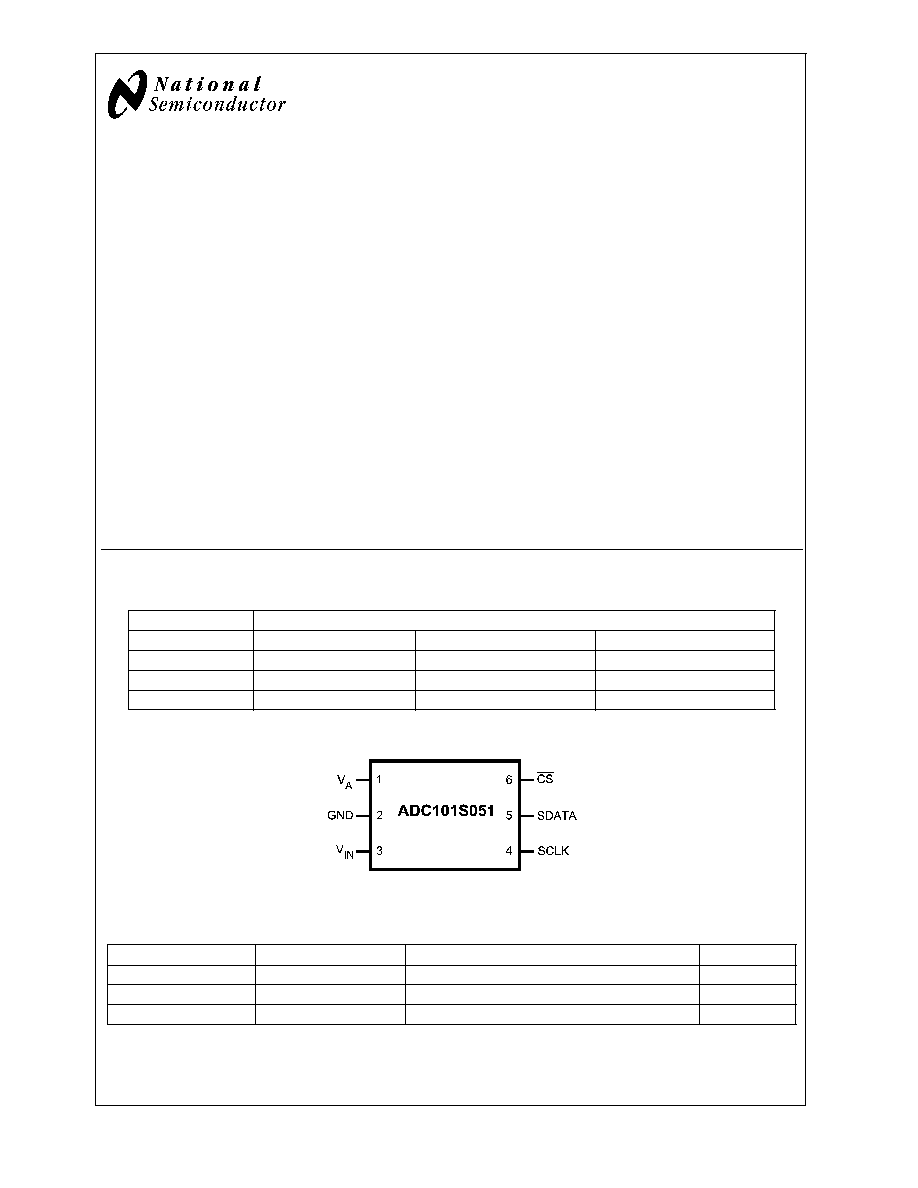
Connection Diagram
20144705
Ordering Information
Order Code
Temperature Range
Description
Top Mark
ADC101S051CIMF
-40�C to +85�C
6-Lead SOT-23 Package
X14C
ADC101S051CIMFX
-40�C to +85�C
6-Lead SOT-23 Package, Tape & Reel
X14C
ADC101S051EVAL
SOT-23 Evaluation Board
TRI-STATE
�
is a trademark of National Semiconductor Corporation
QSPI
TM
and SPI
TM
are trademarks of Motorola, Inc.
September 2005
ADC101S051
Single
Channel,
500
ksps,
10-Bit
A/D
Converter
� 2005 National Semiconductor Corporation
DS201447
www.national.com
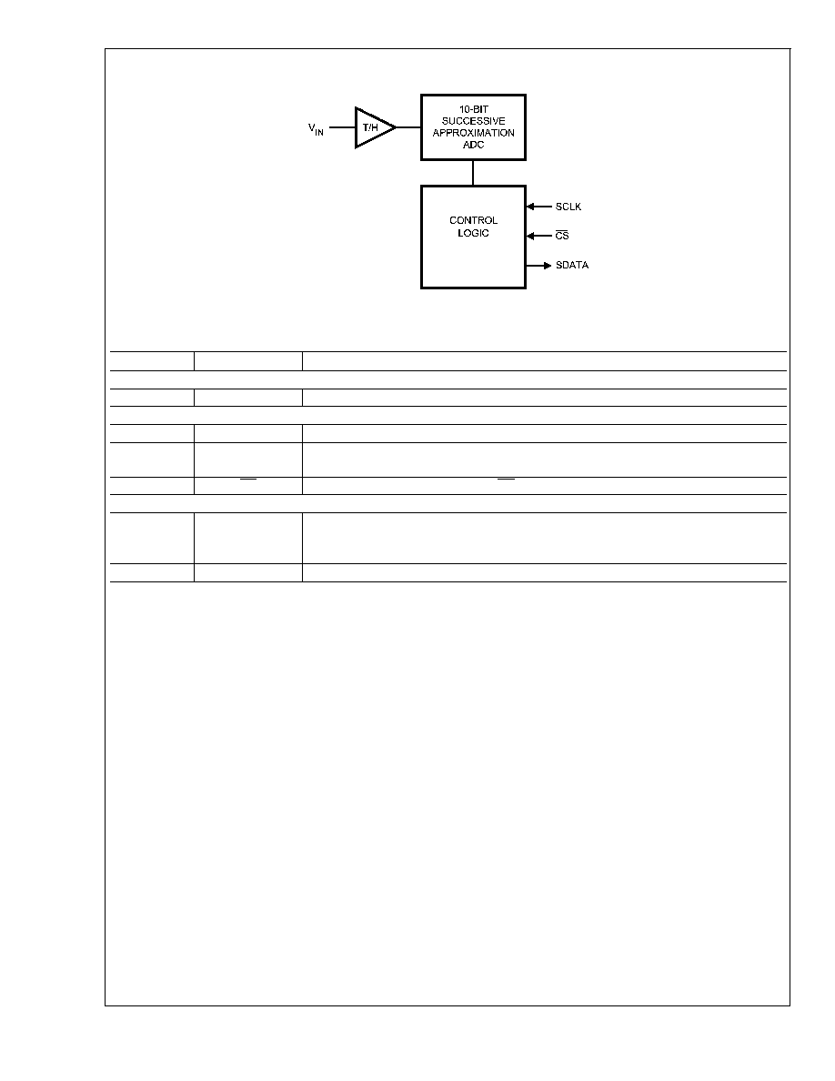
Block Diagram
20144707
Pin Descriptions and Equivalent Circuits
Pin No.
Symbol
Description
ANALOG I/O
3
V
IN
Analog inputs. This signal can range from 0V to V
A
.
DIGITAL I/O
4
SCLK
Digital clock input. This clock directly controls the conversion and readout processes.
5
SDATA
Digital data output. The output samples are clocked out of this pin on falling edges of
the SCLK pin.
6
CS
Chip select. On the falling edge of CS, a conversion process begins.
POWER SUPPLY
1
V
A
Positive supply pin. This pin should be connected to a quiet +2.7V to +5.25V source
and bypassed to GND with a 1 �F capacitor and a 0.1 �F monolithic capacitor located
within 1 cm of the power pin.
2
GND
The ground return for the supply and signals.
ADC101S051
www.national.com
2
Absolute Maximum Ratings
(Notes 1, 2)
If Military/Aerospace specified devices are required,
please contact the National Semiconductor Sales Office/
Distributors for availability and specifications.
Analog Supply Voltage V
A
-0.3V to 6.5V
Voltage on Any Analog Pin to GND
-0.3V to (V
A
+0.3V)
Voltage on Any Digital Pin to GND
-0.3V to 6.5V
Input Current at Any Pin (Note 3)
�
10 mA
Package Input Current (Note 3)
�
20 mA
Power Consumption at T
A
= 25�C
See (Note 4)
ESD Susceptibility (Note 5)
Human Body Model
Machine Model
3500V
300V
Junction Temperature
+150�C
Storage Temperature
-65�C to +150�C
Operating Ratings
(Notes 1, 2)
Operating Temperature Range
-40�C
T
A
+85�C
V
A
Supply Voltage
+2.7V to +5.25V
Digital Input Pins Voltage Range
(regardless of supply voltage)
-0.3V to 5.25V
Analog Input Pins Voltage Range
0V to V
A
Clock Frequency
1 MHz to 10 MHz
Sample Rate
up to 500 kSPS
Package Thermal Resistance
Package
JA
6-lead SOT-23
265�C / W
Soldering process must comply with National Semiconduc-
tor's Reflow Temperature Profile specifications. Refer to
www.national.com/packaging. (Note 6)
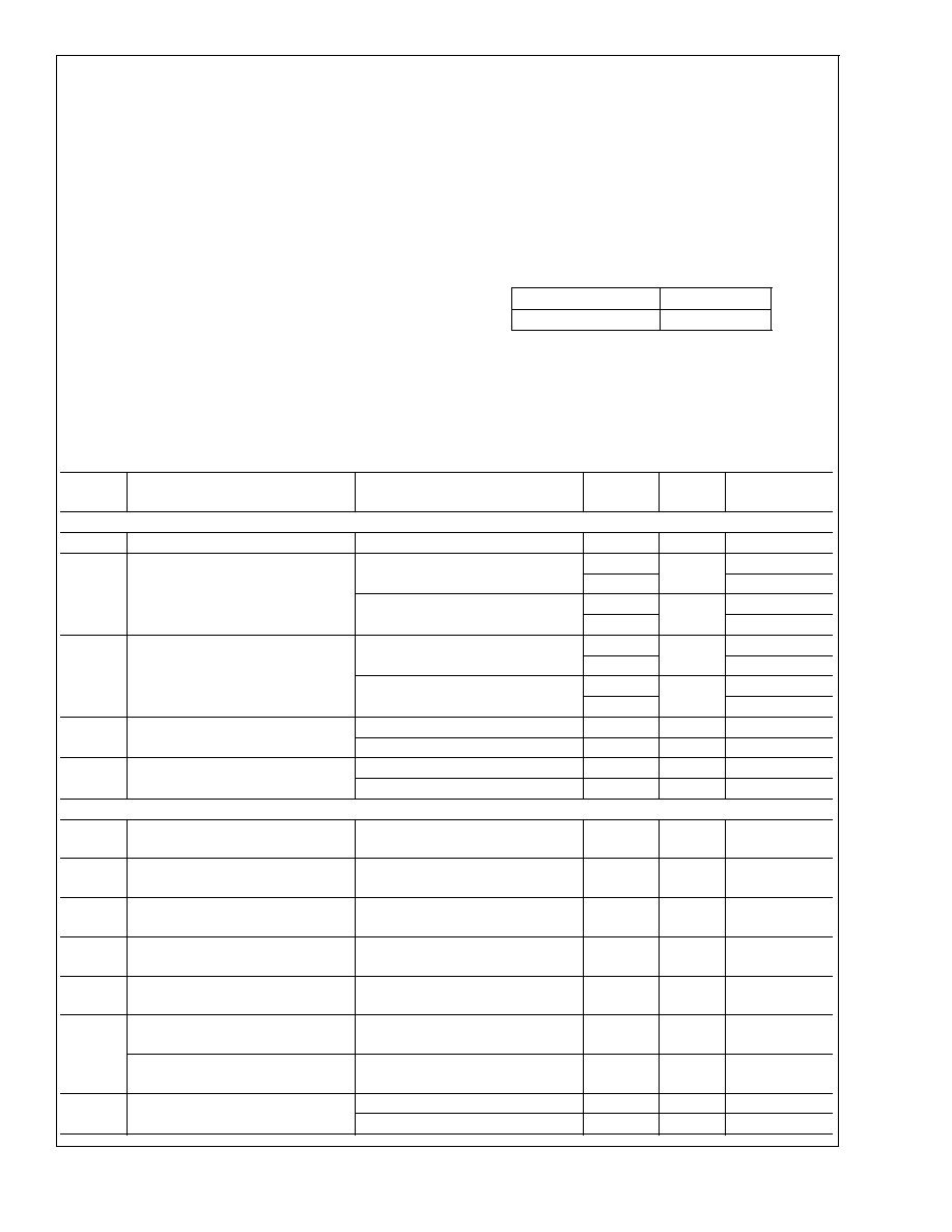
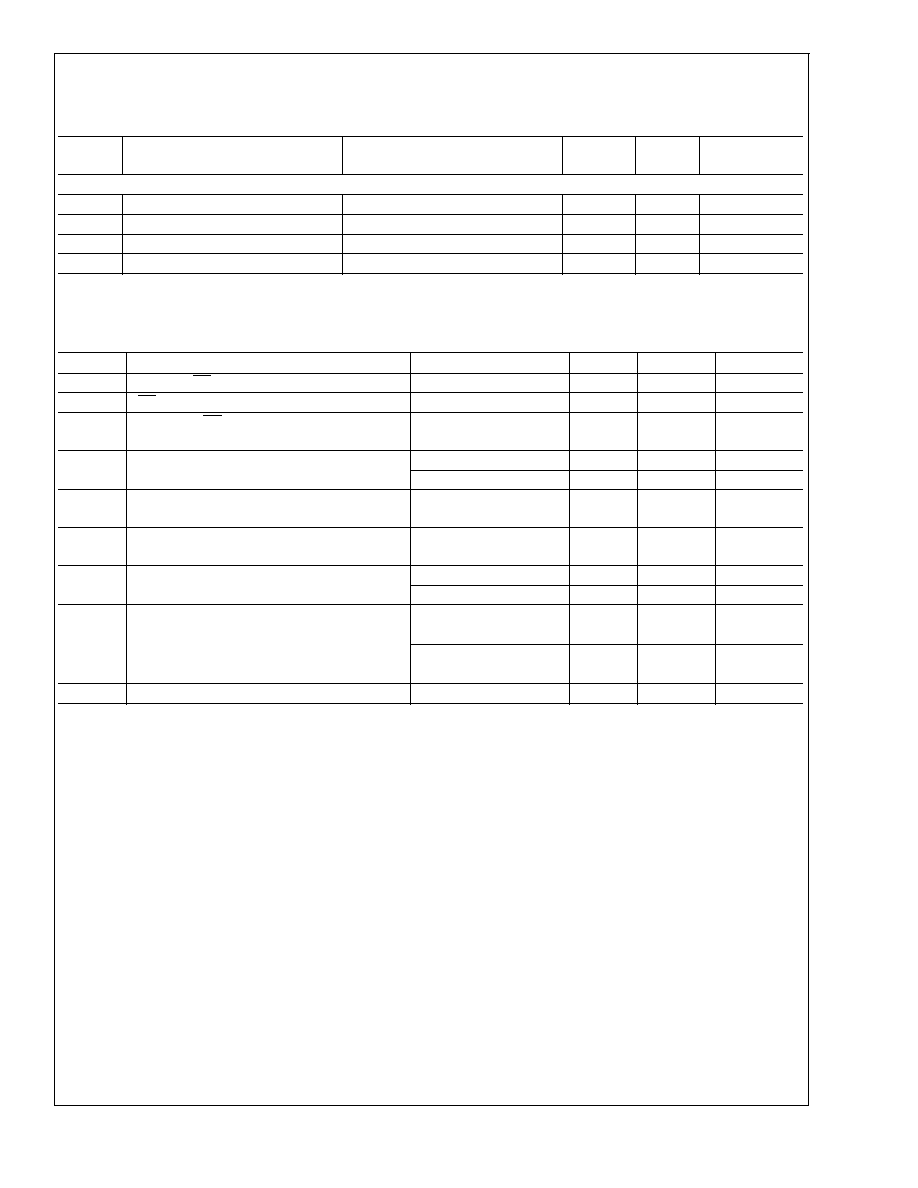
ADC101S051 Converter Electrical Characteristics
(Note 9)
The following specifications apply for V
A
= +2.7V to 5.25V, GND = 0V, f
SCLK
= 4 MHz to 10 MHz, C
L
= 25 pF,
f
SAMPLE
= 200 kSPS to 500 kSPS , unless otherwise noted. Boldface limits apply for T
A
= T
MIN
to T
MAX
: all other limits T
A
=
25�C.
Symbol
Parameter
Conditions
Typical
Limits
(Note 9)
Units
STATIC CONVERTER CHARACTERISTICS
Resolution with No Missing Codes
10
Bits
INL
Integral Non-Linearity
V
A
= +2.7 to +3.6V
+0.12
�
0.7
LSB (max)
-0.08
LSB (min)
V
A
= +4.75 to +5.25V
+0.15
�
0.7
LSB (max)
-0.09
LSB (min)
DNL
Differential Non-Linearity
V
A
= +2.7 to +3.6V
+0.15
�
0.7
LSB (max)
-0.11
LSB (min)
V
A
= +4.75 to +5.25V
+0.15
�
0.7
LSB (max)
-0.11
LSB (min)
V
OFF
Offset Error
V
A
= +2.7 to +3.6V
+0.21
�
0.7
LSB (max)
V
A
= +4.75 to +5.25V
+0.11
�
0.7
LSB (max)
GE
Gain Error
V
A
= +2.7 to +3.6V
-0.2
�
1.0
LSB (max)
V
A
= +4.75 to +5.25V
-0.33
�
1.0
LSB (max)
DYNAMIC CONVERTER CHARACTERISTICS
SINAD
Signal-to-Noise Plus Distortion Ratio
V
A
= +2.7 to 5.25V
f
IN
= 100 kHz, -0.02 dBFS
61.5
60.8
dB (min)
SNR
Signal-to-Noise Ratio
V
A
= +2.7 to 5.25V
f
IN
= 100 kHz, -0.02 dBFS
61.6
61
dB (min)
THD
Total Harmonic Distortion
V
A
= +2.7 to 5.25V
f
IN
= 100 kHz, -0.02 dBFS
-78
-72.5
dB (max)
SFDR
Spurious-Free Dynamic Range
V
A
= +2.7 to 5.25V
f
IN
= 100 kHz, -0.02 dBFS
79
74
dB (min)
ENOB
Effective Number of Bits
V
A
= +2.7 to 5.25V
f
IN
= 100 kHz, -0.02 dBFS
9.9
9.8
Bits (min)
IMD
Intermodulation Distortion, Second
Order Terms
V
A
= +5.25V
f
a
= 104.3 kHz, f
b
= 113.5 kHz
-83
dB
Intermodulation Distortion, Third
Order Terms
V
A
= +5.25V
f
a
= 104.3 kHz, f
b
= 113.5 kHz
-82
dB
FPBW
-3 dB Full Power Bandwidth
V
A
= +5V
11
MHz
V
A
= +3V
8
MHz
ADC101S051
www.national.com
3
ADC101S051 Converter Electrical Characteristics
(Note 9) (Continued)
The following specifications apply for V
A
= +2.7V to 5.25V, GND = 0V, f
SCLK
= 4 MHz to 10 MHz, C
L
= 25 pF,
f
SAMPLE
= 200 kSPS to 500 kSPS , unless otherwise noted. Boldface limits apply for T
A
= T
MIN
to T
MAX
: all other limits T
A
=
25�C.
Symbol
Parameter
Conditions
Typical
Limits
(Note 9)
Units
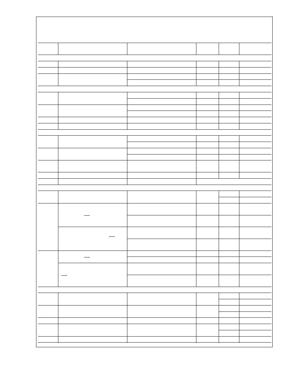
ANALOG INPUT CHARACTERISTICS
V
IN
Input Range
0 to V
A
V
I
DCL
DC Leakage Current
�
1
�A (max)
C
INA
Input Capacitance
Track Mode
30
pF
Hold Mode
4
pF
DIGITAL INPUT CHARACTERISTICS
V
IH
Input High Voltage
V
A
= +5.25V
2.4
V (min)
V
A
= +3.6V
2.1
V (min)
V
IL
Input Low Voltage
V
A
= +5V
0.8
V (max)
V
A
= +3V
0.4
V (max)
I
IN
Input Current
V
IN
= 0V or V
A
�
0.1
�
1
�A (max)
C
IND
Digital Input Capacitance
2
4
pF (max)
DIGITAL OUTPUT CHARACTERISTICS
V
OH
Output High Voltage
I
SOURCE
= 200 �A
V
A
- 0.07
V
A
- 0.2
V (min)
I
SOURCE
= 1 mA
V
A
- 0.1
V
V
OL
Output Low Voltage
I
SINK
= 200 �A
0.03
0.4
V (max)
I
SINK
= 1 mA
0.1
V
I
OZH
,
I
OZL
TRI-STATE
�
Leakage Current
�
0.1
�
10
�A (max)
C
OUT
TRI-STATE
�
Output Capacitance
2
4
pF (max)
Output Coding
Straight (Natural) Binary
POWER SUPPLY CHARACTERISTICS (C
L
= 10 pF)
V
A
Supply Voltage
2.7
V (min)
5.25
V (max)
I
A
Supply Current, Normal Mode
(Operational, CS low)
V
A
= +5.25V,
f
SAMPLE
= 200 kSPS
1.85
2.6
mA (max)
V
A
= +3.6V,
f
SAMPLE
= 200 kSPS
0.75
1.2
mA (max)
Supply Current, Shutdown (CS high)
f
SCLK
= 0 MHz, V
A
= +5.25V
f
SAMPLE
= 0 kSPS
0.5
�A
V
A
= +5.25V, f
SCLK
= 10 MHz,
f
SAMPLE
= 0 kSPS
21
�A
P
D
Power Consumption, Normal Mode
(Operational, CS low)
V
A
= +5.25V
9.7
13.7
mW (max)
V
A
= +3.6V
2.7
4.3
mW (max)
Power Consumption, Shutdown
(CS high)
f
SCLK
= 0 MHz, V
A
= +5.25V
f
SAMPLE
= 0 kSPS
2.6
�W
V
A
= +5.25V, f
SCLK
= 10 MHz,
f
SAMPLE
= 0 kSPS
110
�W
AC ELECTRICAL CHARACTERISTICS
f
SCLK
Clock Frequency
(Note 8)
4
MHz (min)
10
MHz (max)
f
S
Sample Rate
(Note 8)
200
kSPS (min)
500
kSPS (max)
t
CONV
Conversion Time
16
SCLK cycles
DC
SCLK Duty Cycle
f
SCLK
= 10 MHz
50
40
% (min)
60
% (max)
t
ACQ
Track/Hold Acquisition Time
400
ns (max)
ADC101S051
www.national.com
4
ADC101S051 Converter Electrical Characteristics
(Note 9) (Continued)
The following specifications apply for V
A
= +2.7V to 5.25V, GND = 0V, f
SCLK
= 4 MHz to 10 MHz, C
L
= 25 pF,
f
SAMPLE
= 200 kSPS to 500 kSPS , unless otherwise noted. Boldface limits apply for T
A
= T
MIN
to T
MAX
: all other limits T
A
=
25�C.
Symbol
Parameter
Conditions
Typical
Limits
(Note 9)
Units
AC ELECTRICAL CHARACTERISTICS
Throughput Time
Acquisition Time + Conversion Time
20
SCLK cycles
t
QUIET
(Note 10)
50
ns (min)
t
AD
Aperture Delay
3
ns
t
AJ
Aperture Jitter
30
ps
ADC101S051 Timing Specifications
The following specifications apply for V
A
= +2.7V to 5.25V, GND = 0V, f
SCLK
= 4 MHz to 10 MHz, C
L
= 25 pF,
f
SAMPLE
= 200 kSPS to 500 kSPS, Boldface limits apply for T
A
= T
MIN
to T
MAX
: all other limits T
A
= 25�C.
Symbol
Parameter
Conditions
Typical
Limits
Units
t
CS
Minimum CS Pulse Width
10
ns (min)
t
SU
CS to SCLK Setup Time
10
ns (min)
t
EN
Delay from CS Until SDATA TRI-STATE
�
Disabled (Note 11)
20
ns (max)
t
ACC
Data Access Time after SCLK Falling Edge
(Note 12)
V
A
= +2.7V to +3.6V
40
ns (max)
V
A
= +4.75V to +5.25V
20
ns (max)
t
CL
SCLK Low Pulse Width
0.4 x
t
SCLK
ns (min)
t
CH
SCLK High Pulse Width
0.4 x
t
SCLK
ns (min)
t
H
SCLK to Data Valid Hold Time
V
A
= +2.7V to +3.6V
7
ns (min)
V
A
= +4.75V to +5.25V
5
ns (min)
t
DIS
SCLK Falling Edge to SDATA High
Impedance (Note 13)
V
A
= +2.7V to +3.6V
25
ns (max)
6
ns (min)
V
A
= +4.75V to +5.25V
25
ns (max)
6
ns (min)
t
POWER-UP
Power-Up Time from Full Power-Down
1
�s
Note 1: Absolute Maximum Ratings indicate limits beyond which damage to the device may occur. Operating Ratings indicate conditions for which the device is
functional, but do not guarantee specific performance limits. For guaranteed specifications and test conditions, see the Electrical Characteristics. The guaranteed
specifications apply only for the test conditions listed. Some performance characteristics may degrade when the device is not operated under the listed test
conditions.
Note 2: All voltages are measured with respect to GND = 0V, unless otherwise specified.
Note 3: When the input voltage at any pin exceeds the power supply (that is, V
IN
<
GND or V
IN
>
V
A
), the current at that pin should be limited to 10 mA. The 20
mA maximum package input current rating limits the number of pins that can safely exceed the power supplies with an input current of 10 mA to two. The Absolute
Maximum Rating specification does not apply to the V
A
pin. The current into the V
A
pin is limited by the Analog Supply Voltage specification.
Note 4: The absolute maximum junction temperature (T
J
max) for this device is 150�C. The maximum allowable power dissipation is dictated by T
J
max, the
junction-to-ambient thermal resistance (
JA
), and the ambient temperature (T
A
), and can be calculated using the formula P
D
MAX = (T
J
max - T
A
)/
JA
. The values
for maximum power dissipation listed above will be reached only when the device is operated in a severe fault condition (e.g. when input or output pins are driven
beyond the power supply voltages, or the power supply polarity is reversed). Obviously, such conditions should always be avoided.
Note 5: Human body model is 100 pF capacitor discharged through a 1.5 k
resistor. Machine model is 220 pF discharged through zero ohms
Note 6: Reflow temperature profiles are different for lead-free and non-lead-free packages.
Note 7: Tested limits are guaranteed to National's AOQL (Average Outgoing Quality Level).
Note 8: This is the frequency range over which the electrical performance is guaranteed. The device is functional over a wider range which is specified under
Operating Ratings.
Note 9: Datasheet min/max specification limits are guaranteed by design, test, or statistical analysis.
Note 10: Minimum Quiet Time required by bus relinquish and the start of the next conversion.
Note 11: Measured with the timing test circuit shown in Figure 1 and defined as the time taken by the output signal to cross 1.0V.
Note 12: Measured with the timing test circuit shown in Figure 1 and defined as the time taken by the output signal to cross 1.0V going low or 2.0V going high.
Note 13: t
DIS
is derived from the time taken by the outputs to change by 0.5V with the timing test circuit shown in Figure 1. The measured number is then adjusted
to remove the effects of charging or discharging the load capacitance. This means that t
DIS
is the true bus relinquish time, independent of the bus loading.
ADC101S051
www.national.com
5