ADC121S625
12-Bit, 50 ksps to 200 ksps, Differential Input, Micro
Power Sampling A/D Converter
General Description
The ADC121S625 is a 12-bit, 50 ksps to 200 ksps sampling
Analog-to-Digital (A/D) converter that features a fully differ-
ential, high impedance analog input and an external refer-
ence. While best performance is achieved with reference
voltage between 500mV and 2.5V, the reference voltage can
be varied from 100mV to 2.5V, with a corresponding resolu-
tion between 49µV and 1.22mV.
The output serial data is binary 2's complement, and is
compatible with several standards, such as SPI
TM
, QSPI
TM
,
MICROWIRE
TM
, and with many common DSP serial inter-
faces. The differential input, low power, automatic power
down, and small size make the ADC121S625 ideal for direct
connection to transducers in battery operated systems or
remote data acquisition applications.
Operating from a single +5V supply, the normal power con-
sumption is reduced to a few nanowatts in the power-down
mode. The ADC121S625 is a pin-compatible superior re-
placement for the ADS7817 and is available in the MSOP-8
package. Operation is guaranteed over the industrial tem-
perature range of -40∞C to +85∞C and clock rates of 800 kHz
to 3.2 MHz.
Features
n
True Differential Inputs
n
Guaranteed performance from 50ksps to 200ksps
n
External Reference
n
High AC Common-Mode Rejection
n
SPI
TM
/QSPI
TM
/MICROWIRE
TM
/DSP compatible Serial
Interface
Key Specifications
n
Conversion Rate
50 to 200 ksps
n
Offset Error
0.4 LSB (typ)
n
Gain Error
0.05 LSB (typ)
n
INL
±
1 LSB (max)
n
DNL
±
0.75 LSB (max)
n
CMRR
82 dB (typ)
n
Power Consumption
--
Active, 200ksps
2.25 mW (typ)
--
Active, 50ksps
1.33 mW (typ)
--
Power Down
60 nW (typ)
Applications
n
Automotive Navigation
n
Portable Systems
n
Medical Instruments
n
Instrumentation and Control Systems
n
Motor Control
n
Direct Sensor Interface
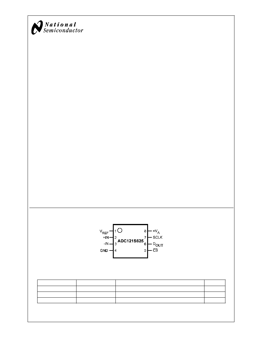
Connection Diagram
20132705
Ordering Information
Order Code
Temperature Range
Description
Top Mark
ADC121S625CIMM
-40∞C to +85∞C
8-Lead MSOP Package, 1000 Units Tape & Reel
X0AC
ADC121S625CIMMX
-40∞C to +85∞C
8-Lead MSOP Package, 3500 Units Tape & Reel
X0AC
ADC121S625EVAL
Evaluation Board
TRI-STATE
Æ
is a trademark of National Semiconductor Corporation.
MICROWIRE
TM
is a trademark of National Semiconductor Corporation.
QSPI
TM
and SPI
TM
are trademarks of Motorola, Inc.
May 2005
ADC121S625
12-Bit,
50
ksps
to
200
ksps,
Differential
Input,
Micro
Power
Sampling
A/D
Converter
© 2005 National Semiconductor Corporation
DS201327
www.national.com
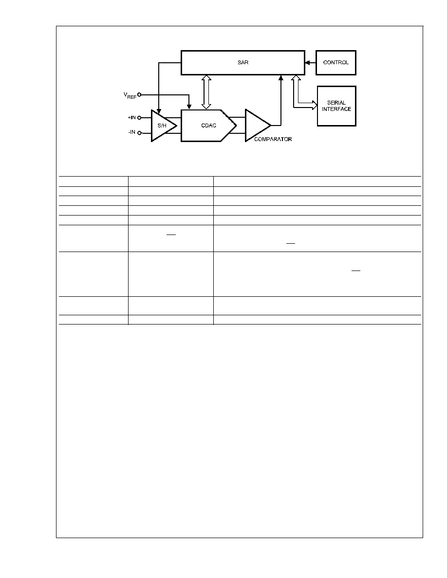
Block Diagram
20132702
Pin Descriptions and Equivalent Circuits
Pin No.
Symbol
Description
1
V
REF
Reference Voltage input.
2
+IN
Non-inverting input.
3
-IN
Inverting input.
4
GND
Ground pin.
5
CS
The ADC is in the active move when this pin is LOW and in
the Power-Down Mode when this pin is HIGH. A conversion
begins at the fall of CS.
6
D
OUT
The serial output data word is comprised of 12 bits of data. In
operation the data is valid on the falling edge of SCLK. The
second clock pulse after the falling edge of CS enables the
serial output. After one null bit the data is valid for the next 12
SCLK edges.
7
SCLK
Serial Clock used to control data transfer. Also serves as the
conversion clock.
8
V
A
Power Supply input.
ADC121S625
www.national.com
2

Absolute Maximum Ratings
(Notes 1, 2)
If Military/Aerospace specified devices are required,
please contact the National Semiconductor Sales Office/
Distributors for availability and specifications.
Analog Supply Voltage V
A
-0.3V to 6.5V
Voltage on Any Pin to GND
-0.3V to (V
A
+0.3V)
Input Current at Any Pin (Note 3)
±
10 mA
Package Input Current (Note 3)
±
50 mA
Power Consumption at T
A
= 25∞C
See (Note 4)
ESD Susceptibility (Note 5)
Human Body Model
Machine Model
2500V
250V
Charge Device Modeling (CDM)
750V
Soldering Temperature, Infrared,
10 seconds (Note 6)
260∞C
Junction Temperature
+150∞C
Storage Temperature
-65∞C to +150∞C
Operating Ratings
(Notes 1, 2)
Operating Temperature Range
-40∞C
T
A
+85∞C
Supply Voltage, V
A
+4.5V to +5.5V
Reference Voltage, V
REF
+0.1V to 2.5V
Input Common-Mode Voltage,
V
CM
See Figure 1 (Sect 2.3)
Digital Input Pins Voltage Range
0 to V
A
Clock Frequency
0.8 MHz to 3.2 MHz
Differential Analog Input Voltage
-V
REF
to +V
REF
Package Thermal Resistance
Package
JA
8-lead MSOP
20∞C / W
ADC121S625 Converter Electrical Characteristics
(Note 8)
The following specifications apply for V
A
= +4.5V to 5.5V, V
REF
= 2.5V, f
SCLK
= 0.8 to 3.2 MHz, f
IN
= 20 kHz, C
L
= 100 pF, un-
less otherwise noted. Boldface limits apply for T
A
= T
MIN
to T
MAX
: all other limits T
A
= 25∞C.
Symbol
Parameter
Conditions
Typical
Limits
Units
(Note 7)
STATIC CONVERTER CHARACTERISTICS
Resolution with No Missing Codes
12
Bits
INL
Integral Non-Linearity
+0.5
-0.3
+1.0
-1.0
LSB (max)
LSB (min)
DNL
Differential Non-Linearity
±
0.4
±
0.75
LSB (max)
OE
Offset Error
0.4
±
4
LSB (max)
FSE
Positive Full-Scale Error
+0.2
LSB
Negative Full-Scale Error
+0.2
LSB
GE
Gain Error
-0.05
±
4
LSB
DYNAMIC CONVERTER CHARACTERISTICS
SINAD
Signal-to-Noise Plus Distortion Ratio
f
IN
= 20 kHz, -0.1 dBFS
72.6
68.5
dBc (min)
SNR
Signal-to-Noise Ratio
f
IN
= 20 kHz, -0.1 dBFS
72.9
70
dBc (min)
THD
Total Harmonic Distortion
f
IN
= 20 kHz, -0.1 dBFS
-84
-74
dBc (max)
SFDR
Spurious-Free Dynamic Range
f
IN
= 20 kHz, -0.1 dBFS
85.2
74
dBc (min)
ENOB
Effective Number of Bits
f
IN
= 20 kHz, -0.1 dBFS
11.8
11.1
bits (min)
FPBW
-3 dB Full Power Bandwidth
Output at 70.7%FS
with FS Input
Differential
Input
26
MHz
Single-Ended
Input
22
MHz
ANALOG INPUT CHARACTERISTICS
V
IN
Differential Input Range
-V
REF
V (min)
+V
REF
V (max)
I
DCL
DC Leakage Current
±
0.04
±
2
µA (max)
C
INA
Input Capacitance
In Track Mode
17
pF
In Hold Mode
3
pF
CMRR
Common Mode Rejection Ratio
82
dB
V
REF
Reference Voltage Range
0.1
V (min)
2.5
V (max)
ADC121S625
www.national.com
3

ADC121S625 Converter Electrical Characteristics
(Note 8) (Continued)
The following specifications apply for V
A
= +4.5V to 5.5V, V
REF
= 2.5V, f
SCLK
= 0.8 to 3.2 MHz, f
IN
= 20 kHz, C
L
= 100 pF, un-
less otherwise noted. Boldface limits apply for T
A
= T
MIN
to T
MAX
: all other limits T
A
= 25∞C.
Symbol
Parameter
Conditions
Typical
Limits
Units
(Note 7)
ANALOG INPUT CHARACTERISTICS
I
REF
Reference Current
CS low, f
SCLK
= 3.2 MHz,
f
S
= 200 ksps, output = FF8h
12
µA
CS low, f
SCLK
= 3.2 MHz,
f
S
= 50 ksps, output = FF8h
3
µA
CS low, f
SCLK
= 3.2 MHz,
12.5 ksps, output = FF8h
0.7
µA
CS high, f
SCLK
= 0
0.3
µA
DIGITAL INPUT CHARACTERISTICS
V
IH
Input High Voltage
V
A
= 4.5V to 5.5V
2.4
V (min)
V
IL
Input Low Voltage
V
A
= 4.5V to 5.5V
0.8
V (max)
I
IN
Input Current
V
IN
= 0V or V
A
±
0.03
1
µA (max)
C
IND
Input Capacitance
2
4
pF (max)
DIGITAL OUTPUT CHARACTERISTICS
V
OH
Output High Voltage
V
A
= 4.5V to 5.5V, I
SOURCE
= 250 µA
V
A
- 0.05
V
A
- 0.2
V (min)
V
A
= 4.5V to 5.5V, I
SOURCE
= 2 mA
V
A
- 0.1
V
V
OL
Output Low Voltage
V
A
= 4.5V to 5.5V, I
SINK
= 250 µA
0.02
0.4
V (max)
V
A
= 4.5V to 5.5V, I
SOURCE
= 2 mA
0.1
V
I
OZH
,
I
OZL
TRI-STATE Leakage Current
±
0.03
±
1
µA (max)
C
OUT
TRI-STATE Output Capacitance
2
4
pF (max)
Output Coding
Binary 2'S Complement
POWER SUPPLY CHARACTERISTICS
V
A
Analog Supply Voltage
4.5
V (min)
5.5
V (max)
I
A
Active
Supply Current, Normal Mode
(Operational)
f
SCLK
= 3.2 MHz, f
SMPL
= 200 ksps,
f
IN
= 20 kHz, C
L
= 15pF
410
510
µA (max)
f
SCLK
= 3.2 MHz, f
SMPL
= 12.5 ksps,
C
L
= 15pF, Power Down between
conversions
31
µA
f
SCLK
= 0.8 MHz, f
SMPL
= 50 ksps,
C
L
= 15pF
242
µA
f
SCLK
= 0.2 MHz, f
SMPL
= 12.5 ksps,
C
L
= 15pF (Note 10)
200
µA
I
A
Shutdown
Supply Current, Shutdown (CS high)
f
SCLK
= 0
0.01
2
µA (max)
f
SCLK
= 3.2 MHz
6
µA
PWR
Active
Power Consumption, Normal Mode
(Operational)
f
SCLK
= 3.2 MHz, f
SMPL
= 200 ksps,
f
IN
= 20 kHz, C
L
= 15pF
2.25
2.8
mW (max)
f
SCLK
= 3.2 MHz, f
SMPL
= 12.5 ksps,
C
L
= 15pF, Power Down between
conversions
0.18
mW
f
SCLK
= 0.8 MHz, f
SMPL
= 50 ksps,
C
L
= 15pF
1.33
mW
f
SCLK
= 0.2 MHz, f
SMPL
= 12.5 ksps,
C
L
= 15pF (Note 10)
1.1
mW
PWR
Shutdown
Power Consumption, Shutdown (CS
high)
f
SCLK
= 0
0.06
11
µW (max)
f
SCLK
= 3.2 MHz
33
µW
ADC121S625
www.national.com
4

ADC121S625 Converter Electrical Characteristics
(Note 8) (Continued)
The following specifications apply for V
A
= +4.5V to 5.5V, V
REF
= 2.5V, f
SCLK
= 0.8 to 3.2 MHz, f
IN
= 20 kHz, C
L
= 100 pF, un-
less otherwise noted. Boldface limits apply for T
A
= T
MIN
to T
MAX
: all other limits T
A
= 25∞C.
Symbol
Parameter
Conditions
Typical
Limits
Units
(Note 7)
POWER SUPPLY CHARACTERISTICS
PSRR
Power Supply Rejection Ratio
Offset Change with 1.0V change in
V
A
71
dB
Gain Error Change with 1.0V change
in V
A
83
dB
AC ELECTRICAL CHARACTERISTICS
f
SCLK
Maximum Clock Frequency
4.8
3.2
MHz (min)
f
SCLK
Minimum Clock Frequency
200
800
kHz (max)
f
S
Maximum Sample Rate
300
200
ksps (min)
t
ACQ
Track/Hold Acquisition Time
1.5
SCLK cycles
(min)
2.0
SCLK cycles
(max)
t
CONV
Conversion Time
12
12
SCLK cycles
t
CYC
Throughput Time
Normal Operation
16
SCLK cycles
Short Cycled
14
SCLK cycles
(min)
f
RATE
Throughput Rate
200
ksps (max)
t
AD
Aperture Delay
6
ns
ADC121S625 Timing Specifications
(Note 8)
The following specifications apply for V
A
= +4.5V to 5.5V, V
REF
= 2.5V, f
SCLK
= 0.8 MHz to 3.2 MHz, C
L
= 100 pF, Boldface
limits apply for T
A
= T
MIN
to T
MAX
: all other limits T
A
= 25∞C.
Symbol
Parameter
Conditions
Typical
Limits
Units
t
CFCS
SCLK Fall toCS Fall
0
ns (min)
t
CSCR
CS Fall to SCLK Rise
(Note 9)
0
ns (min)
t
CHLD
SCLK Fall to Data Change Hold Time
(Note 9)
10
ns (min)
t
CDV
SCLK Fall to Next D
OUT
Valid
38
100
ns (max)
t
DIS
Rising Edge of CS To D
OUT
Disabled
38
50
ns (max)
t
EN
2nd SCLK Fall after CS Fall to D
OUT
Enabled
6
50
ns (max)
t
CH
SCLK High Time
42
60
ns (min)
t
CL
SCLK Low Time
42
60
ns (min)
t
r
D
OUT
Rise Time
5
50
ns (max)
t
f
D
OUT Fall Time
13
50
ns (max)
Note 1: Absolute maximum ratings are limiting values which indicate limits beyond which damage to the device may occur. Operating Ratings indicate conditions
for which the device is functional, but do not guarantee specific performance limits. For guaranteed specifications and test conditions, see the Electrical
Characteristics. The guaranteed specifications apply only for the test conditions listed. Some performance characteristics may degrade when the device is not
operated under the listed test conditions.
Note 2: All voltages are measured with respect to GND = 0V, unless otherwise specified.
Note 3: When the input voltage at any pin exceeds the power supplies (that is, V
IN
<
AGND or V
IN
>
V
A
or V
D
), the current at that pin should be limited to 10 mA.
The 50 mA maximum package input current rating limits the number of pins that can safely exceed the power supplies with an input current of 10 mA to five.
Note 4: The absolute maximum junction temperature (T
J
max) for this device is 150∞C. The maximum allowable power dissipation is dictated by T
J
max, the
junction-to-ambient thermal resistance (
JA
), and the ambient temperature (T
A
), and can be calculated using the formula P
D
MAX = (T
J
max - T
A
)/
JA
. The values
for maximum power dissipation listed above will be reached only when the ADC121S625 is operated in a severe fault condition (e.g. when input or output pins are
driven beyond the power supply voltages, or the power supply polarity is reversed). Obviously, such conditions should always be avoided.
Note 5: Human body model is 100 pF capacitor discharged through a 1.5 k
resistor. Machine model is 220 pF discharged through ZERO ohms.
Note 6: See AN450, "Surface Mounting Methods and Their Effect on Product Reliability", or the section entitled "Surface Mount" found in any post 1986 National
Semiconductor Linear Data Book, for other methods of soldering surface mount devices.
Note 7: Tested limits are guaranteed to National's AOQL (Average Outgoing Quality Level).
Note 8: Data sheet min/max specification limits are guaranteed by design, test, or statistical analysis.
Note 9: Clock should be in low when CS is asserted, as indicated by the t
CSCR
and t
CFCS
specifications.
Note 10: While the maximum sample rate is f
SCLK
/16, the actual sample rate may be lower than this by having the CS rate being slower than f
SCLK
/16.
ADC121S625
www.national.com
5