
ADC12D040
Dual 12-Bit, 40 MSPS, 600 mW A/D Converter with
Internal/External Reference and Sample-and-Hold
General Description
The ADC12D040 is a dual, low power monolithic CMOS
analog-to-digital converter capable of converting analog in-
put signals into 12-bit digital words at 40 Megasamples per
second (MSPS), minimum. This converter uses a differential,
pipelined architecture with digital error correction and an
on-chip sample-and-hold circuit to minimize die size and
power consumption while providing excellent dynamic per-
formance. Operating on a single 5V power supply, the
ADC12D040 achieves 10.9 effective bits at 10 MHz input
and consumes just 600 mW at 40 MSPS, including the
reference current. The Power Down feature reduces power
consumption to 75 mW.
The differential inputs provide a full scale input swing equal
to V
REF
with the possibility of a single-ended input. Full use
of the differential input is recommended for optimum perfor-
mance. For ease of use, the buffered, high impedance,
single-ended reference input is converted on-chip to a differ-
ential reference for use by the processing circuitry. The
digital outputs for the two ADCs are available on separate
12-bit buses with an output data format choice of offset
binary or 2's complement.
For ease of interface, the digital output driver power pins of
the ADC12D040 can be connected to a separate supply
voltage in the range of 2.5V to the digital supply voltage,
making the outputs compatible with low voltage systems.
When not converting, power consumption can be reduced by
pulling the PD pin high, placing the converter into the power-
down state where it typically consumes just 75 mW. The
ADC12D040's speed, resolution and single supply operation
make it well suited for a variety of applications.
This device is available in the 64-lead TQFP package and
will operate over the industrial temperature range of -40∞C to
+85∞C.
Features
n
Binary/2's comp output format
n
Single supply operation
n
Internal sample-and-hold
n
Outputs 2.5V to 5V compatible
n
TTL/CMOS compatible input/outputs
n
Low power consumption
n
Power down mode
n
On-chip reference buffer
n
Internal/External 2V reference
Key Specifications
n
Resolution
12 Bits
n
Conversion Rate
40 MSPS(min)
n
DNL
±
0.4 LSB(typ)
n
INL
±
0.7 LSB(typ)
n
SNR (f
IN
= 10MHz)
68 dB(typ)
n
ENOB (f
IN
= 10MHz)
10.9 bits(typ)
n
THD (f
IN
= 10 MHz)
-78 dB (typ)
n
SFDR (f
IN
= 10 MHz)
80 dB (typ)
n
Data Latency
6 Clock Cycles
n
Supply Voltage
+5V
±
5%
n
Power Consumption, Operating
600 mW(typ)
n
Power Down
75 mW(typ)
n
Crosstalk
80 dB(typ)
Applications
n
Ultrasound and Imaging
n
Instrumentation
n
Communications Receivers
n
Sonar/Radar
n
xDSL
n
Cable Modems
n
DSP Front Ends
December 2002
ADC12D040
Dual
12-Bit,
40
MSPS,
600
mW
A/D
Converter
with
Internal/External
Reference
and
Sample-and-Hold
© 2002 National Semiconductor Corporation
DS200460
www.national.com
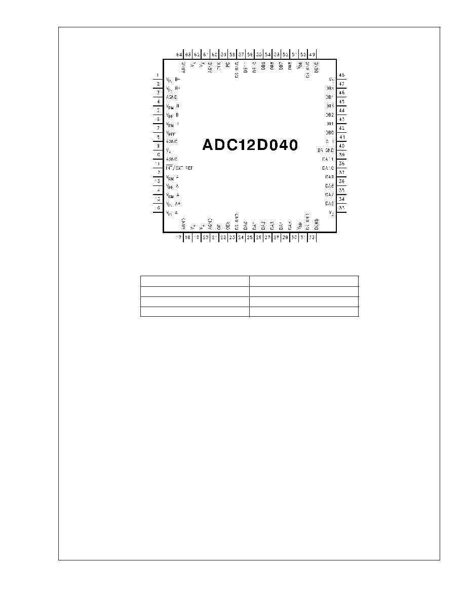
Connection Diagram
20046001
Ordering Information
Industrial (-40∞C
T
A
+85∞C)
Package
ADC12D040CIVS
64 Pin TQFP
ADC12D040CIVSX
64 Pin TQFP Tape and Reel
ADC12D040EVAL
Evaluation Board
ADC12D040
www.national.com
2

Block Diagram
20046002
ADC12D040
www.national.com
3
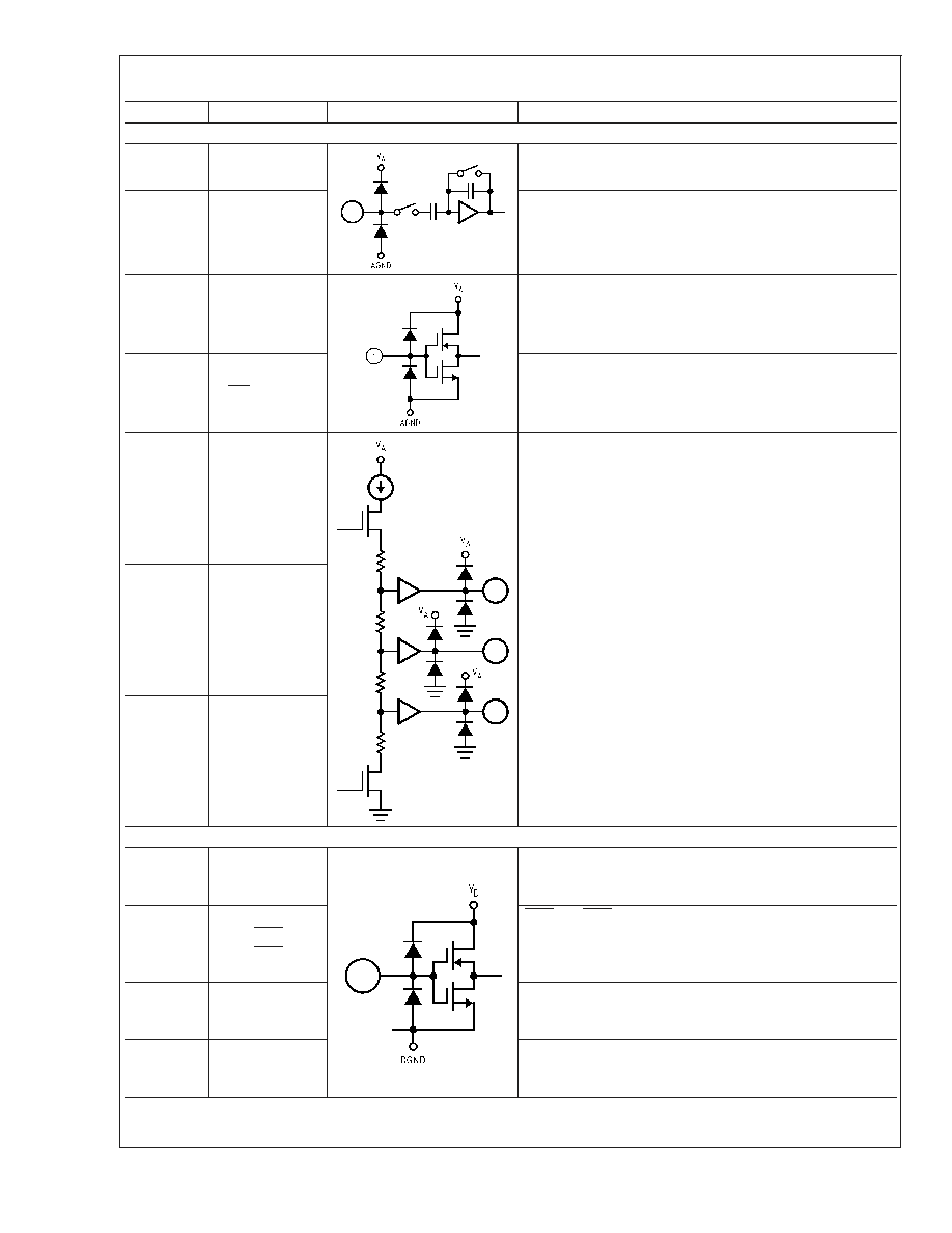
Pin Descriptions and Equivalent Circuits
Pin No.
Symbol
Equivalent Circuit
Description
ANALOG I/O
15
2
V
INA+
V
INB+
Non-Inverting analog signal Inputs. With a 2.0V reference
voltage each input signal level is 2.0 V
P-P
centered on V
CM
.
16
1
V
INA-
V
INB-
Inverting analog signal Input. With a 2.0V reference voltage
the input signal level is from 2.0 V
P-P
centered on V
CM
. This
pin may be connected to V
CM
for single-ended operation, but
a differential input signal is required for best performance.
7
V
REF
Reference input. This pin should be bypassed to AGND with
a 0.1 µF monolithic capacitor. V
REF
is 2.0V nominal and
should be between 1.0V to 2.4V.
11
INT/EXT REF
V
REF
select pin. With a logic low at this pin the internal 2.0V
reference is selected. With a logic high on this pin an external
reference voltage should be applied to V
REF
input pin 7.
13
5
V
RPA
V
RPB
These pins are high impedance reference bypass pins only.
Connect a 0.1 µF capacitor from each of these pins to AGND.
DO NOT connect anything else to these pins.
12
6
V
RNA
V
RNB
14
4
V
RMA
V
RMB
DIGITAL I/O
60
CLK
Digital clock input. The range of frequencies for this input is
100 kHz to 50 MHz (typical) with guaranteed performance at
40 MHz. The input is sampled on the rising edge of this input.
22
41
OEA
OEB
OEA and OEB are the output enable pins that, when low,
enables their respective TRI-STATE data output pins. When
either of these pins is high, the corresponding outputs are in a
high impedance state.
59
PD
PD is the Power Down input pin. When high, this input puts
the converter into the power down mode. When this pin is
low, the converter is in the active mode.
21
OF
Output Format pin. A logic low on this pin causes output data
to be in straight binary. A logic high on this pin causes the
output data to be in 2's complement format.
ADC12D040
www.national.com
4

Pin Descriptions and Equivalent Circuits
(Continued)
Pin No.
Symbol
Equivalent Circuit
Description
24≠29
34≠39
DA0≠DA11
Digital data output pins that make up the 12-bit conversion
results of their respective converters. DA0 and DB0 are the
LSBs, while DA11 and DB11 are the MSBs of the output
word. Output levels are TTL/CMOS compatible.
42≠47
52≠57
DB0≠DB11
ANALOG POWER
9, 18, 19,
62, 63
V
A
Positive analog supply pins. These pins should be connected
to a quiet +5V source and bypassed to AGND with 0.1 µF
monolithic capacitors located within 1 cm of these power pins,
and with a 10 µF capacitor.
3, 8, 10,
17, 20, 61,
64
AGND
The ground return for the analog supply.
DIGITAL POWER
33, 48
V
D
Positive digital supply pin. This pin should be connected to
the same quiet +5V source as is V
A
and be bypassed to
DGND with a 0.1 µF monolithic capacitor located within 1 cm
of the power pin and with a 10 µF capacitor.
32, 49
DGND
The ground return for the digital supply.
30, 51
V
DR
Positive digital supply pins for the ADC12D040's output
drivers. These pins should be connected to a voltage source
of +2.5V to +5V and bypassed to DR GND with a 0.1 µF
monolithic capacitor. If the supply for these pins are different
from the supply used for V
A
and V
D
, they should also be
bypassed with a 10 µF tantalum capacitor. V
DR
should never
exceed the voltage on V
D
. All bypass capacitors should be
located within 1 cm of the supply pin.
23, 31, 40,
50, 58
DR GND
The ground return for the digital supply for the ADC12D040's
output drivers. These pins should be connected to the system
digital ground, but not be connected in close proximity to the
ADC12D040's DGND or AGND pins. See Section 5 (Layout
and Grounding) for more details.
ADC12D040
www.national.com
5