
ADC12L063
12-Bit, 62 MSPS, 354 mW A/D Converter with Internal
Sample-and-Hold
General Description
The ADC12L063 is a monolithic CMOS analog-to-digital con-
verter capable of converting analog input signals into 12-bit
digital words at 62 Megasamples per second (MSPS), mini-
mum. This converter uses a differential, pipelined architec-
ture with digital error correction and an on-chip sample-and-
hold circuit to minimize die size and power consumption
while providing excellent dynamic performance. Operating
on a single 3.3V power supply, this device consumes just
354 mW at 62 MSPS, including the reference current. The
Power Down feature reduces power consumption to just 50
mW.
The differential inputs provide a full scale input swing equal
to
±
V
REF
with the possibility of a single-ended input. Full use
of the differential input is recommended for optimum perfor-
mance. For ease of use, the buffered, high impedance,
single-ended reference input is converted on-chip to a differ-
ential reference for use by the processing circuitry. Output
data format is 12-bit offset binary.
This device is available in the 32-lead LQFP package and
will operate over the industrial temperature range of -40∞C to
+85∞C.
Features
n
Single supply operation
n
Low power consumption
n
Power down mode
n
On-chip reference buffer
Key Specifications
n
Resolution
12 Bits
n
Conversion Rate
62 MSPS(min)
n
Bandwidth
170MHz
n
DNL
±
0.5 LSB(typ)
n
INL
±
1.0 LSB(typ)
n
SNR
66 dB(typ)
n
SFDR
78 dB(typ)
n
Data Latency
6 Clock Cycles
n
Supply Voltage
+3.3V
±
300 mV
n
Power Consumption, 62 MHz
354 mW(typ)
Applications
n
Ultrasound and Imaging
n
Instrumentation
n
Cellular Base Stations/Communications Receivers
n
Sonar/Radar
n
xDSL
n
Wireless Local Loops
n
Data Acquisition Systems
n
DSP Front Ends
Connection Diagram
20026301
November 2002
ADC12L063
12-Bit,
62
MSPS,
354
mW
A/D
Converter
with
Internal
Sample-and-Hold
© 2002 National Semiconductor Corporation
DS200263
www.national.com

Ordering Information
Industrial (-40∞C
T
A
+85∞C)
Package
ADC12L063CIVY
32 Pin LQFP
ADC12L063CIVYX
32 Pin LQFP Tape and Reel
ADC12L063EVAL
Evaluation Board
Block Diagram
20026302
ADC12L063
www.national.com
2
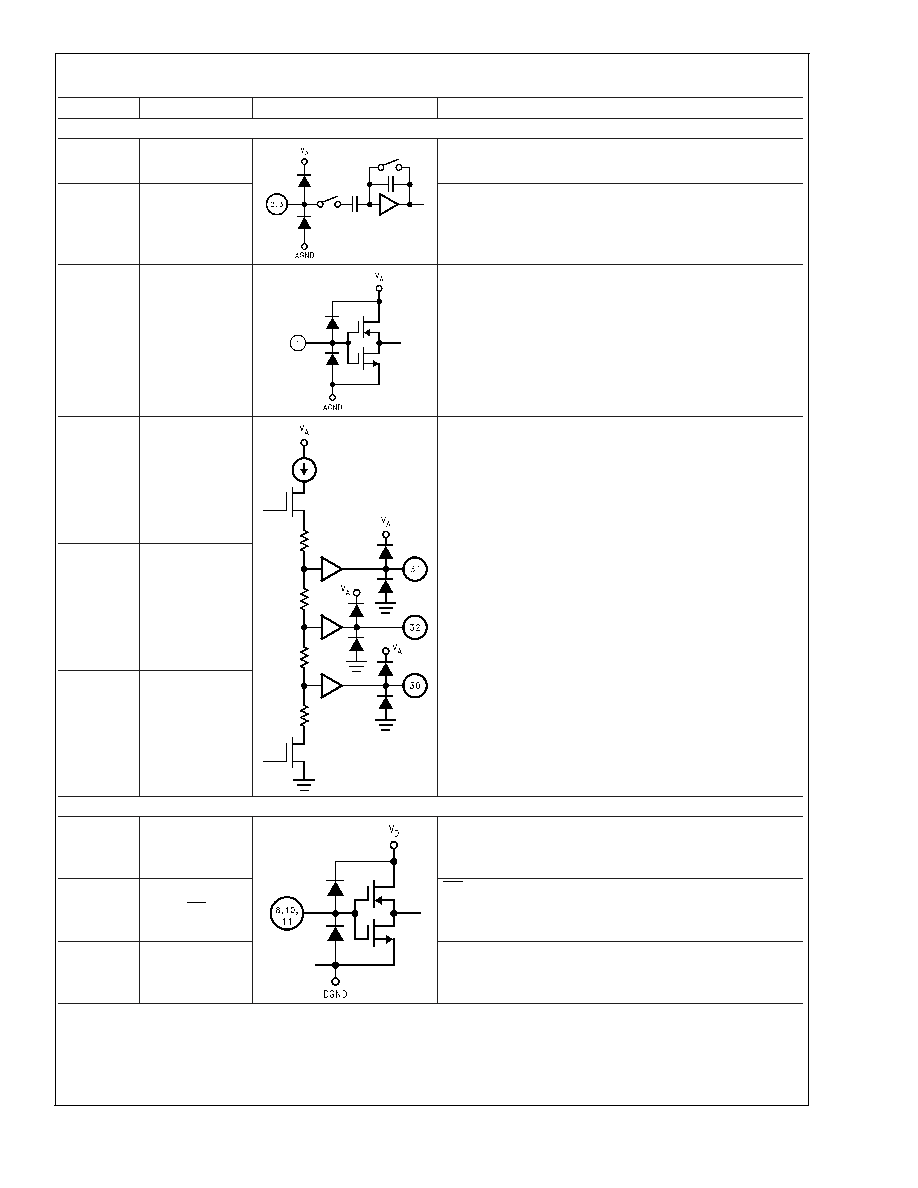
Pin Descriptions and Equivalent Circuits
Pin No.
Symbol
Equivalent Circuit
Description
ANALOG I/O
2
V
IN+
Non-Inverting analog signal Input. With a 1.0V reference
voltage the input signal level is 1.0 V
P-P
.
3
V
IN-
Inverting analog signal Input. With a 1.0V reference voltage
the input signal level is 1.0 V
P-P
. This pin may be connected
to V
CM
for single-ended operation, but a differential input
signal is required for best performance.
1
V
REF
Reference input. This pin should be bypassed to AGND with
a 0.1 µF monolithic capacitor. V
REF
is 1.0V nominal and
should be between 0.8V and 1.2V.
31
V
RP
These pins are high impedance reference bypass pins only.
Connect a 0.1 µF capacitor from each of these pins to AGND.
DO NOT connect anything else to these pins.
32
V
RM
30
V
RN
DIGITAL I/O
10
CLK
Digital clock input. The range of frequencies for this input is 1
MHz to 70 MHz (typical) with guaranteed performance at 62
MHz. The input is sampled on the rising edge of this input.
11
OE
OE is the output enable pin that, when low, enables the
TRI-STATE data output pins. When this pin is high, the
outputs are in a high impedance state.
8
PD
PD is the Power Down input pin. When high, this input puts
the converter into the power down mode. When this pin is
low, the converter is in the active mode.
ADC12L063
www.national.com
3
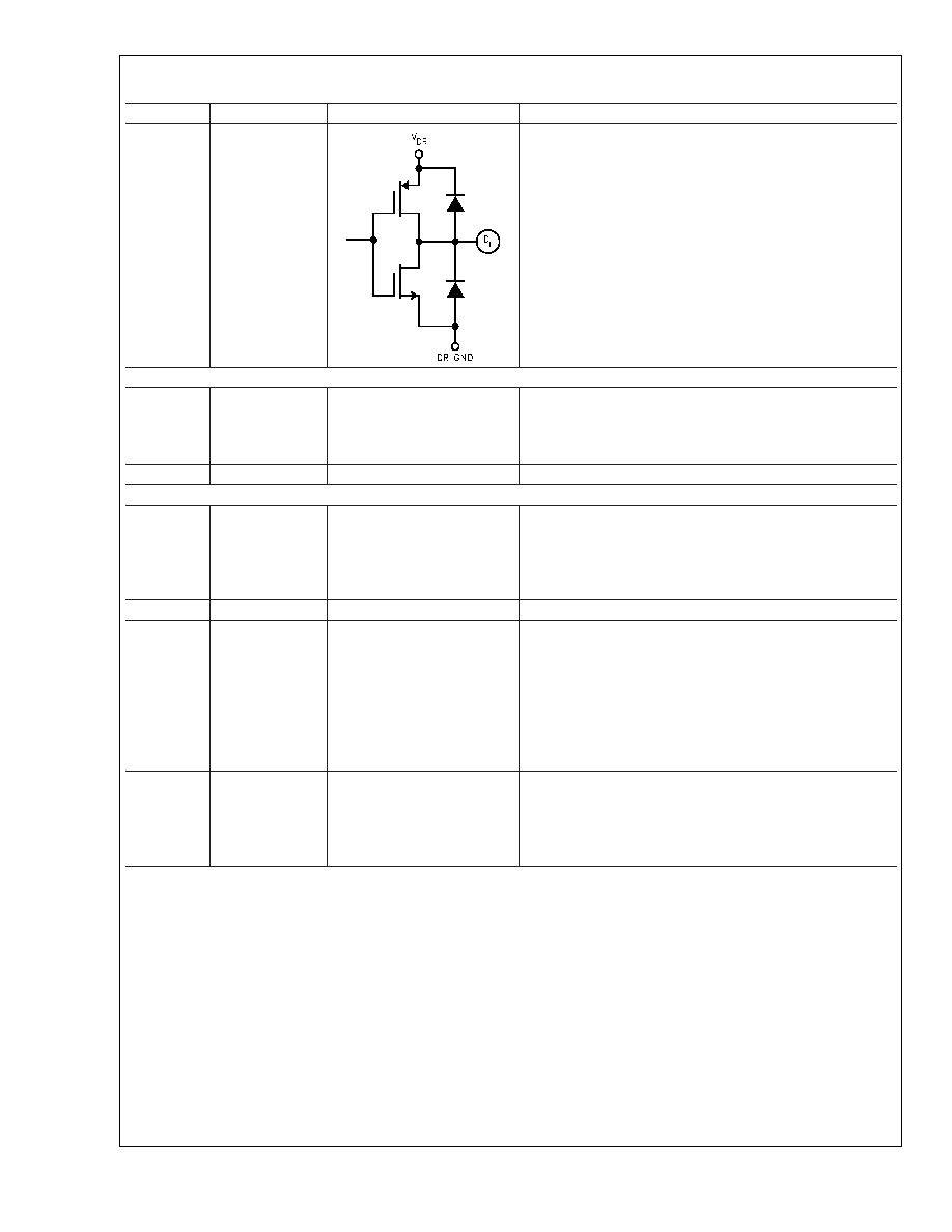
Pin Descriptions and Equivalent Circuits
(Continued)
Pin No.
Symbol
Equivalent Circuit
Description
14≠19,
22≠27
D0≠D11
Digital data output pins that make up the 12-bit conversion
results. D0 is the LSB, while D11 is the MSB of the offset
binary output word.
ANALOG POWER
5, 6, 29
V
A
Positive analog supply pins. These pins should be connected
to a quiet +3.3V source and bypassed to AGND with 0.1 µF
monolithic capacitors located within 1 cm of these power pins,
and with a 10 µF capacitor.
4, 7, 28
AGND
The ground return for the analog supply.
DIGITAL POWER
13
V
D
Positive digital supply pin. This pin should be connected to
the same quiet +3.3V source as is V
A
and bypassed to
DGND with a 0.1 µF monolithic capacitor in parallel with a 10
µF capacitor, both located within 1 cm of the power pin.
Decouple this pin from the V
A
pins.
9, 12
DGND
The ground return for the digital supply.
21
V
DR
Positive digital supply pin for the ADC12L063's output drivers.
This pin should be connected to a voltage source of +2.5V to
V
D
and bypassed to DR GND with a 0.1 µF monolithic
capacitor. If the supply for this pin is different from the supply
used for V
A
and V
D
, it should also be bypassed with a 10 µF
tantalum capacitor. The voltage at this pin should never
exceed the voltage on V
D
. All bypass capacitors should be
located within 1 cm of the supply pin.
20
DR GND
The ground return for the digital supply for the ADC12L063's
output drivers. This pin should be connected to the system
digital ground, but not be connected in close proximity to the
ADC12L063's DGND or AGND pins. See Section 5.0 (Layout
and Grounding) for more details.
ADC12L063
www.national.com
4
Absolute Maximum Ratings
(Notes 1,
2)
If Military/Aerospace specified devices are required,
please contact the National Semiconductor Sales Office/
Distributors for availability and specifications.
V
A
, V
D
, V
DR
4.2V
|V
A
≠V
D
|
100 mV
Voltage on Any Input or Output Pin
-0.3V to V
A
or V
D
+0.3V
Input Current at Any Pin (Note 3)
±
25 mA
Package Input Current (Note 3)
±
50 mA
Package Dissipation at T
A
= 25∞C
See (Note 4)
ESD Susceptibility
Human Body Model (Note 5)
2500V
Machine Model (Note 5)
250V
Soldering Temperature,
Infrared, 10 sec. (Note 6)
235∞C
Storage Temperature
-65∞C to +150∞C
Operating Ratings
(Notes 1, 2)
Operating Temperature
-40∞C
T
A
+85∞C
Supply Voltage (V
A
, V
D
)
+3.0V to +3.60V
Output Driver Supply (V
DR
)
+2.5V to V
D
V
REF
Input
0.8V to 1.2V
CLK, PD, OE
-0.05V to V
D
+ 0.05V
V
IN
Input
-0V to (V
A
- 0.5V)
|AGND≠DGND|
100mV
Converter Electrical Characteristics
Unless otherwise specified, the following specifications apply for AGND = DGND = DR GND = 0V, V
A
= V
D
= V
DR
= +3.3V,
PD = 0V, V
REF
= +1.0V, f
CLK
= 62 MHz, t
r
= t
f
= 2 ns, C
L
= 20 pF/pin. Boldface limits apply for T
A
= T
J
= T
MIN
to T
MAX
: all
other limits T
A
= T
J
= 25∞C (Notes 7, 8, 9)
Symbol
Parameter
Conditions
Typical
(Note 10)
Limits
(Note 10)
Units
(Limits)
STATIC CONVERTER CHARACTERISTICS
Resolution with No Missing Codes
12
Bits
INL
Integral Non Linearity (Note 11)
±
1.0
±
2.4
LSB(max)
DNL
Differential Non Linearity
±
0.5
LSB(max)
GE
Gain Error
Positive Error
-0.8
%FS(max)
Negative Error
+0.1
±
3
%FS(max)
Offset Error (V
IN
+ = V
IN
-)
+0.1
±
0.9
%FS(max)
Under Range Output Code
0
0
Over Range Output Code
4095
4095
REFERENCE AND ANALOG INPUT CHARACTERISTICS
V
CM
Common Mode Input Voltage
1.0
V
C
IN
V
IN
Input Capacitance (each pin to
GND)
V
IN
= 1.0 Vdc
+ 1 V
P-P
(CLK LOW)
8
pF
(CLK HIGH)
7
pF
V
REF
Reference Voltage (Note 13)
1.00
0.8
V(min)
1.2
V(max)
Reference Input Resistance
100
M
(min)
ADC12L063
www.national.com
5