ADC12L080
12-Bit, 80 MSPS, 450 MHz Bandwidth A/D Converter with
Internal Reference
General Description
The ADC12L080 is a monolithic CMOS analog-to-digital con-
verter capable of converting analog input signals into 12-bit
digital words at 80 Megasamples per second (MSPS). This
converter uses a differential, pipeline architecture with digital
error correction and an on-chip sample-and-hold circuit to
minimize die size and power consumption while providing
excellent dynamic performance. The ADC12L080 can be
operated with either the internal or an external reference.
Operating on a single 3.3V power supply, this device con-
sumes just 425 mW at 80 MSPS, including the reference
current. The Power Down feature reduces power consump-
tion to just 50 mW.
The differential inputs provide a full scale input swing equal
to
�
V
REF
. The buffered, high impedance, single-ended ex-
ternal reference input is converted on-chip to a differential
reference for use by the processing circuitry. Output data
format may be selected as either offset binary or two's
complement.
This device is available in the 32-lead LQFP package and
operates over the industrial temperature range of -40�C to
+85�C.
Features
n
Single supply operation
n
Low power consumption
n
Power down mode
n
Internal or external reference
n
Selectable Offset Binary or 2's Complement data format
n
Pin-compatible with ADC12010, ADC12020, ADC12040,
ADC12L063, ADC12L066
Key Specifications
n
Full Power Bandwidth
450 MHz
n
DNL
�
0.4 LSB (typ)
n
SNR (f
IN
= 10 MHz)
66 dB (typ)
n
SFDR (f
IN
= 10 MHz)
80 dB (typ)
n
Power Consumption, 80 MHz
--
Operating
425 mW (typ)
--
Power Down
50 mW (typ)
Applications
n
Ultrasound and Imaging
n
Instrumentation
n
Cellular Base Stations/Communication Receivers
n
Sonar/Radar
n
xDSL
n
Wireless Local Loops
n
Data Acquisition Systems
n
DSP Front Ends
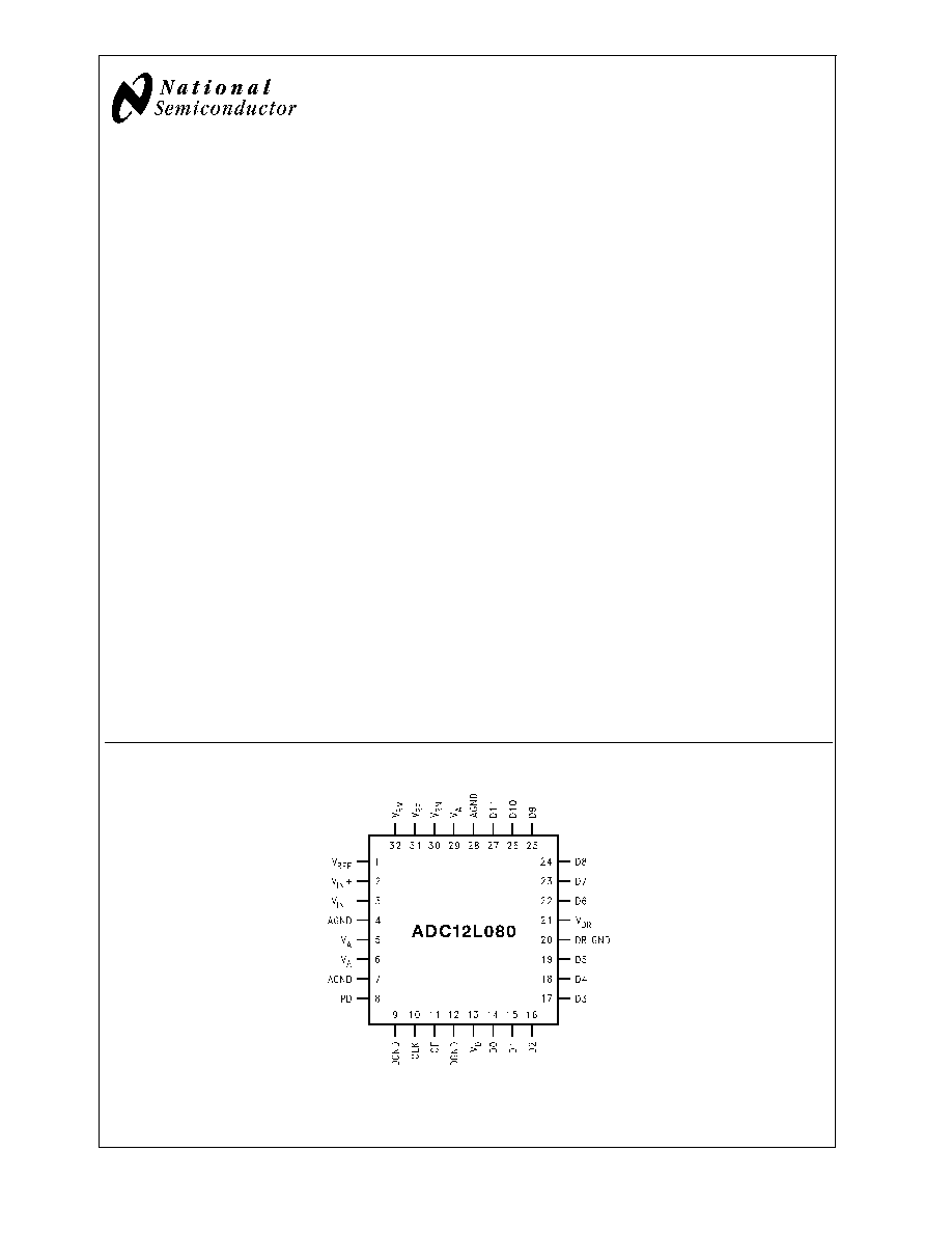
Connection Diagram
20061001
TRI-STATE
�
is a registered trademark of National Semiconductor Corporation.
October 2004
ADC12L080
12-Bit,
80
MSPS,
450
MHz
Bandwidth
A/D
Converter
with
Internal
Reference
� 2004 National Semiconductor Corporation
DS200610
www.national.com

Ordering Information
Industrial (-40�C
T
A
+85�C)
Package
ADC12L080CIVY
32 Pin LQFP
ADC12L080EVAL
Evaluation Board
Block Diagram
20061002
ADC12L080
www.national.com
2
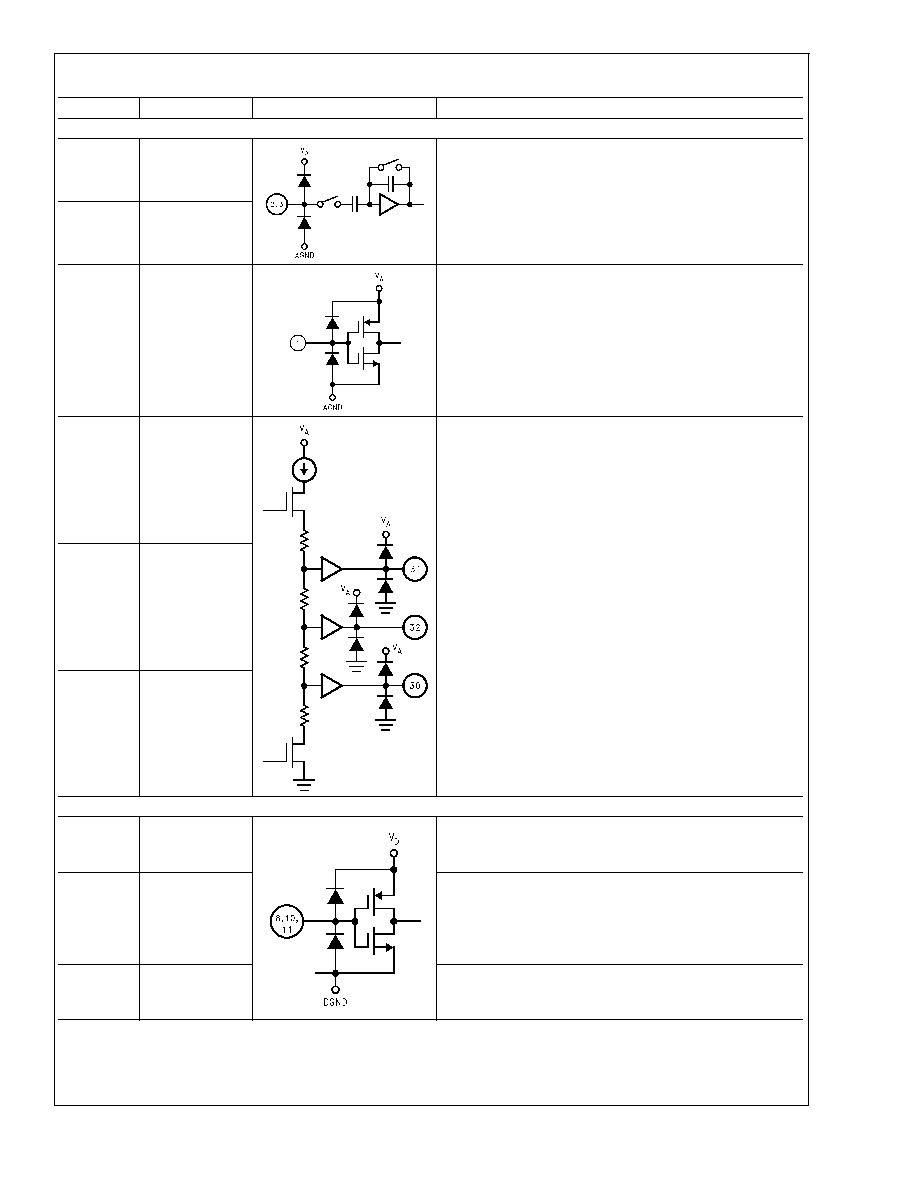
Pin Descriptions and Equivalent Circuits
Pin No.
Symbol
Equivalent Circuit
Description
ANALOG I/O
2
V
IN+
Differential analog signal Input pins. With a 1.0V reference
voltage the full-scale differential input signal level is 2.0 V
P-P
with each input pin centered on a common mode voltage,
V
CM
. The V
IN
- pin may be connected to V
CM
for single-ended
operation, but a differential input signal is required for best
performance.
3
V
IN-
1
V
REF
Reference input. This pin should be connected to V
A
to use
the internal 1.0V reference. If it is desired to use an external
reference voltage, this pin should be bypassed to AGND with
a 0.1 �F low ESL capacitor. Specified operation is with a
V
REF
of 1.0V, but the device will function well with a V
REF
range indicated in the Electrical Tables.
31
V
RP
These pins are high impedance reference bypass pins only.
Connect a 0.1 �F capacitor from each of these pins to AGND.
Connect a 1.0 �F capacitor from V
RP
to V
RN
. DO NOT LOAD
these pins.
32
V
RM
30
V
RN
DIGITAL I/O
10
CLK
Digital clock input. The range of frequencies for this input is
10 MHz to 80 MHz with guaranteed performance at 80 MHz.
The input is sampled on the rising edge of this input.
11
OF
Output format selection. When this pin is LOW, the output
format is offset binary. When this pin is HIGH the output
format is two's complement. This pin may be changed
asynchronously, but such a change will result in errors for one
or two conversions.
8
PD
PD is the Power Down input pin. When high, this input puts
the converter into the power down mode. When this pin is
low, the converter is in the active mode.
ADC12L080
www.national.com
3
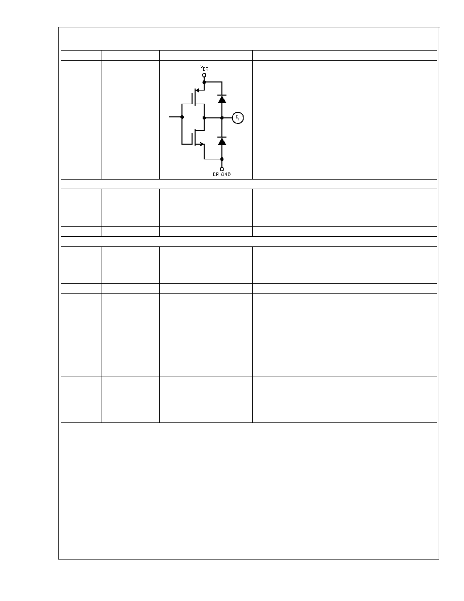
Pin Descriptions and Equivalent Circuits
(Continued)
Pin No.
Symbol
Equivalent Circuit
Description
14�19,
22�27
D0�D11
Digital data output pins that make up the 12-bit conversion
results. D0 is the LSB, while D11 is the MSB of the output
word.
ANALOG POWER
5, 6, 29
V
A
Positive analog supply pins. These pins should be connected
to a quiet +3.3V source and bypassed to AGND with 0.1 �F
low ESL capacitors located within 1 cm of these power pins,
and with a 10 �F capacitor.
4, 7, 28
AGND
The ground return for the analog supply.
DIGITAL POWER
13
V
D
Positive digital supply pin. This pin should be connected to
the same quiet +3.3V source as is V
A
and bypassed to
DGND with a 0.1 �F monolithic capacitor in parallel with a 10
�F capacitor, both located within 1 cm of the power pin.
9, 12
DGND
The ground return for the digital supply.
21
V
DR
Positive digital supply pin for the ADC12L080's output drivers.
This pin should be connected to a voltage source in the range
indicated in the Operating Ratings table and be bypassed to
DR GND with a 0.1 �F capacitor. If the supply for this pin is
different from the supply used for V
A
and V
D
, it should also be
bypassed with a 10 �F capacitor. The voltage at this pin
should never exceed the voltage on V
D
by more than
300 mV. All bypass capacitors should be located within 1 cm
of the supply pin.
20
DR GND
The ground return for the digital supply for the ADC12L080's
output drivers. This pin should be connected to the system
digital ground, but not be connected in close proximity to the
ADC12L080's DGND or AGND pins. See Section 6.0 (Layout
and Grounding) for more details.
ADC12L080
www.national.com
4
Absolute Maximum Ratings
(Notes 1, 2)
If Military/Aerospace specified devices are required,
please contact the National Semiconductor Sales Office/
Distributors for availability and specifications.
V
A
, V
D
, V
DR
4.2V
|V
A
�V
D
|
100 mV
V
DR
�V
D
300 mV
Voltage on Any Pin
-0.3V to V
A
or (V
D
+ 0.3V)
Input Current at Any Pin (Note 3)
�
25 mA
Package Input Current (Note 3)
�
50 mA
Package Dissipation at T
A
= 25�C
See (Note 4)
ESD Susceptibility
Human Body Model (Note 5)
2500V
Machine Model (Note 5)
250V
Soldering Temperature,
Infrared, 10 sec. (Note 6)
235�C
Storage Temperature
-65�C to +150�C
Operating Ratings
(Notes 1, 2)
Operating Temperature
-40�C
T
A
+85�C
Supply Voltage (V
A
, V
D
)
+3.0V to +3.60V
Output Driver Supply (V
DR
)
+2.4V to V
D
V
REF
0.8V to 1.5V
CLK, PD, OF
-0.05V to V
D
+ 0.05V
V
IN
Input
-0V to (V
A
- 0.5V)
V
CM
0.5V to (V
A
-1.5V)
|AGND�DGND|
0V
Package Thermal Resistances
Package
J-A
32-Lead LQFP
79�C / W
Converter Electrical Characteristics
Unless otherwise specified, the following specifications apply for AGND = DGND = DR GND = 0V, V
A
= V
D
= +3.3V, V
DR
=
+2.5V, PD = 0V, V
REF
= +1.0V external, V
CM
= 1.65V, R
S
<
100
, f
CLK
= 80 MHz, t
r
= t
f
= 2 ns, f
IN
= 70 MHz, C
L
= 15 pF/pin.
Boldface limits apply for T
J
= T
MIN
to T
MAX
: all other limits T
J
= 25�C (Notes 7, 8, 9, 10)
Symbol
Parameter
Conditions
Typical
(Note 10)
Limits
(Note 10)
Units
(Limits)
STATIC CONVERTER CHARACTERISTICS
Resolution with No Missing Codes
12
Bits
INL
Integral Non Linearity
Best Fit Method
�
1.2
4.0
LSB (max)
-3.3
LSB (min)
DNL
Differential Non Linearity
No missing codes
�
0.4
1.5
LSB (max)
-1.0
LSB (min)
GE
Gain Error
Positive Error
-0.15
+5.7
-2
%FS (max)
%FS (min)
Negative Error
+0.4
+5
-3.7
%FS (max)
%FS (min)
Offset Error (V
IN
+ = V
IN
-)
+0.2
+1.7
-0.6
%FS (max)
Under Range Output Code
0
0
Over Range Output Code
4095
4095
REFERENCE AND ANALOG INPUT CHARACTERISTICS
V
CM
Common Mode Input Voltage
1.65
0.5
V (min)
2.0
V (max)
C
IN
V
IN
Input Capacitance
(each pin to GND)
V
IN
= 1.0 Vdc
+ 1 V
P-P
(CLK LOW)
8
pF
(CLK HIGH)
7
pF
V
REF
Reference Voltage (Note 12)
1.0
0.8
V (min)
1.5
V (max)
ADC12L080
www.national.com
5